Display panel and display device

A display panel, transition display technology, applied in the direction of identification devices, instruments, electrical components, etc., can solve problems such as interference and screen flickering in the camera area, and achieve the effect of preventing flickering and avoiding interference.

Pending Publication Date: 2021-11-23
WUHAN CHINA STAR OPTOELECTRONICS SEMICON DISPLAY TECH CO LTD
View PDF3 Cites 1 Cited by
  • Summary
  • Abstract
  • Description
  • Claims
  • Application Information

AI Technical Summary

Problems solved by technology

[0004] Embodiments of the present invention provide a display panel and a display device to solve the problem that in the area of ​​the camera under the existing display panel, the infrared light emitted by the emission sensor of the TOF camera will interfere with the transistor device installed above the camera, resulting in Technical issue with screen flickering in the camera area

Method used


Image

  • Display panel and display device
  • Display panel and display device
  • Display panel and display device

Examples


Embodiment Construction

[0045] Next, the technical solutions in the embodiments of the present invention will be described in connection with the drawings of the embodiments of the present invention, and it is understood that the described embodiments are merely the embodiments of the present invention, not all of the embodiments. Based on the embodiments of the present invention, those skilled in the art are in the range of the protected by the present invention without creative labor premistence. Further, it should be understood that the specific embodiments described herein are only to illustrate and explain the present invention and are not intended to limit the present invention. Nouns in the present invention, in the absence of instructions to the contrary, as used "upper" and "lower" generally refers to the upper and lower means in actual use or operation state, in particular direction in the drawing plane of FIG. ; and "inner" and "outer" are terms for the profile of the device.
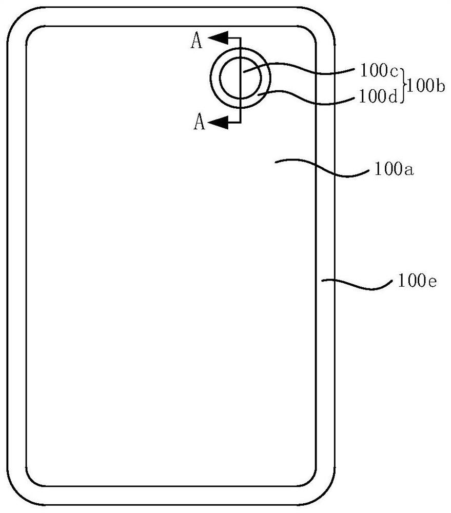
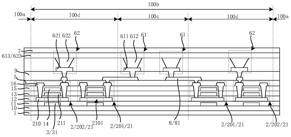
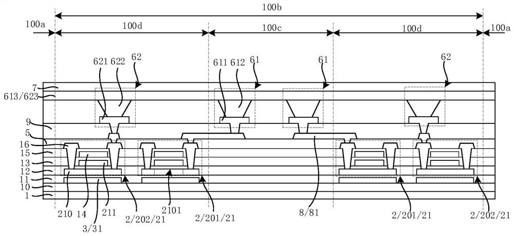
[0046] See figu...


PUM

PropertyMeasurementUnit
Sizeaaaaaaaaaa

Abstract

The invention discloses a display panel and a display device. The display panel comprises a substrate, a plurality of pixel driving circuits and a light shielding layer. Each pixel driving circuit comprises a plurality of transistors, and the orthographic projection of an active layer of each transistor on the substrate and the orthographic projection of a first electrode layer on the substrate have an overlapping part. The light shielding layer is arranged in a transition display area of the display panel and located between the substrate and the active layer of each transistor of the pixel driving circuit, and the orthographic projection of the light shielding part on the substrate covers the orthographic projections of the overlapping parts on the substrate, so that the light shielding layer can effectively shield infrared light emitted by an emission sensor of an optical sensing unit, the interference effect of the infrared light on a transistor device arranged in the transition display area is avoided, and the flicker phenomenon of a camera area under the screen is prevented.

Description

Technical field [0001] The present invention relates to display technology, and particularly relates to a display panel and a display device. Background technique [0002] TOF (Time of Flight, TOF) is the use of optical technology to measure the time of flight distance, has been widely used in areas such as smart phones face recognition, 3D structure compared to the light, it has a detection distance, simple structure advantage. [0003] The way to realize screen camera (Camera Under Panel, CUP) technology is mounted TOF technology transmitting and receiving ends respectively TOF camera placed below the region of the lower two panel camera. However, TOF camera is an infrared laser light source generates an infrared transmitter and receiver to obtain depth information, in practical applications, the infrared light emitted by the transmitter TOF camera be provided over the transistor devices interfere with the camera, so that the screen the lower region of the screen flickers camer...

Claims


Application Information

Patent Timeline
IPC IPC(8): H01L23/552G09F9/33
CPCH01L23/552G09F9/33H01L25/167H01L25/0753H01L33/46H01L33/10H01L33/62
Inventor 杨程江盼
Owner WUHAN CHINA STAR OPTOELECTRONICS SEMICON DISPLAY TECH CO LTD
Why Eureka
Try Eureka