Display panel and display device

A display panel and bias technology, applied to static indicators, instruments, etc., can solve problems such as threshold voltage drift of driving transistors, achieve the effect of weakening threshold voltage drift and ensuring display uniformity

Active Publication Date: 2021-11-26
XIAMEN TIANMA MICRO ELECTRONICS
View PDF9 Cites 0 Cited by
  • Summary
  • Abstract
  • Description
  • Claims
  • Application Information

AI Technical Summary

Problems solved by technology

[0004] Embodiments of the present invention provide a display panel and a display device to improve the threshold voltage drift problem of the existing driving transistor

Method used


Image

  • Display panel and display device
  • Display panel and display device
  • Display panel and display device

Examples


Embodiment Construction

[0046] In order to make the purpose, technical solutions and advantages of the present invention clearer, the technical solutions of the present invention will be clearly and completely described through implementation with reference to the accompanying drawings in the embodiments of the present invention. Obviously, the described embodiments are the embodiment of the present invention. Some, but not all, embodiments. All other embodiments obtained by those skilled in the art based on the basic concepts disclosed and suggested by the embodiments of the present invention belong to the protection scope of the present invention.

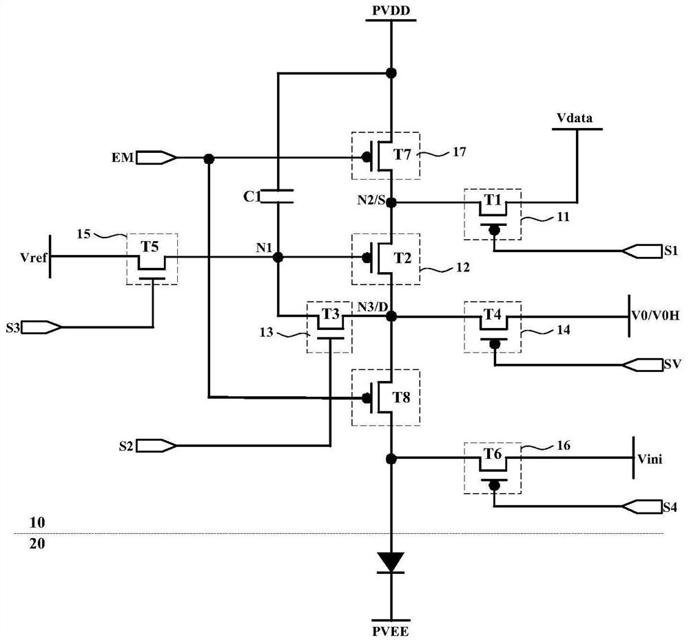
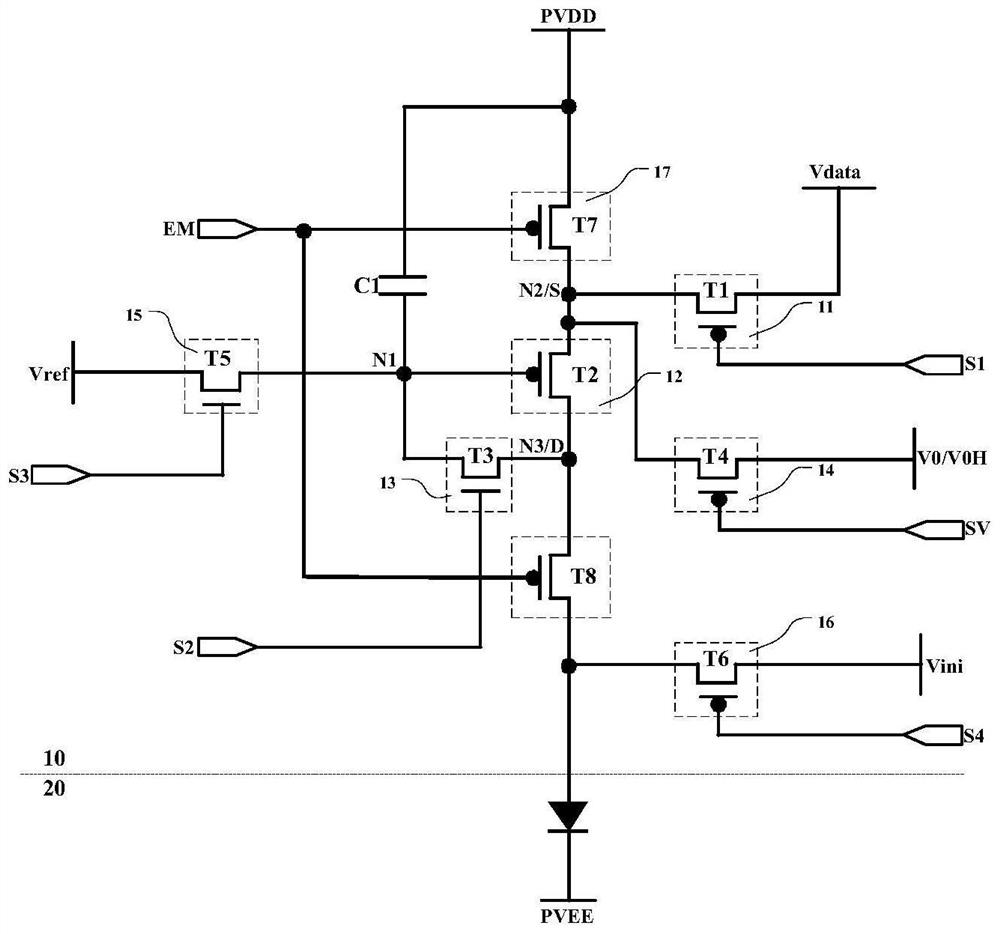
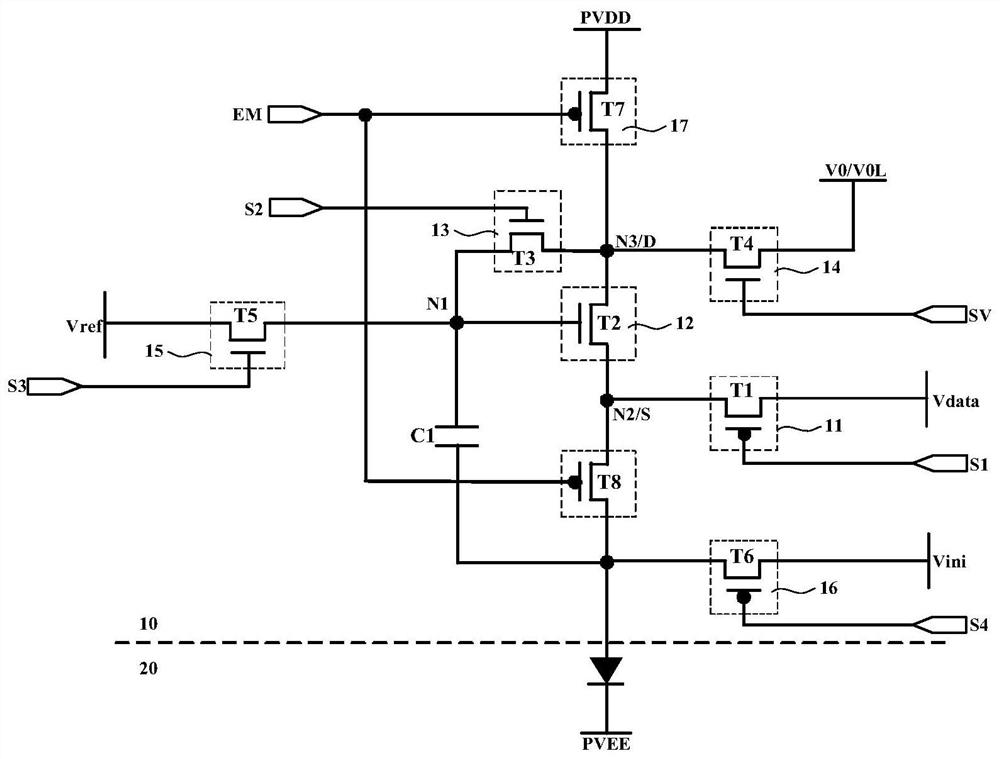
[0047] refer to Figure 1-Figure 4 as shown, figure 1 It is a schematic structural diagram of a pixel circuit of a display panel provided by an embodiment of the present invention, figure 2 A schematic structural diagram of a pixel circuit of another display panel provided by an embodiment of the present invention, image 3 is a schematic structural...


PUM


Abstract

The embodiment of the invention discloses a display panel and a display device. The display panel comprises a pixel circuit and a light-emitting element, the pixel circuit comprises a data writing module, a driving module and a bias adjusting module. The driving module comprises a driving transistor; the data write-in module is connected to the source electrode of the driving transistor; the bias adjusting module is connected between the source electrode or the drain electrode of the driving transistor and a bias adjusting signal end; the working process of the pixel circuit comprises a bias adjusting stage, and in the bias adjusting stage, the bias adjusting module is started to provide a bias adjusting signal for the source electrode or the drain electrode of the driving transistor; the driving transistor is a PMOS (P-channel Metal Oxide Semiconductor), and the bias adjusting signal is a high-level signal, or the driving transistor is an NMOS (N-channel Metal Oxide Semiconductor), and the bias adjusting signal is a low-level signal. In the embodiment of the invention, the bias adjustment stage can balance the threshold voltage drift phenomenon of the driving transistor in the non-bias stage.

Description

technical field [0001] Embodiments of the present invention relate to the field of display technology, and in particular, to a display panel and a display device. Background technique [0002] In the display panel, the pixel circuit provides the driving current for the light-emitting elements of the display panel required for display, and controls whether the light-emitting elements enter the light-emitting stage, and is an indispensable element in most self-luminous display panels. [0003] However, in the existing display panel, as the usage time increases, the internal characteristics of the driving transistor in the pixel circuit change slowly, causing the threshold voltage of the driving transistor to drift, thereby affecting the comprehensive characteristics of the driving transistor, and further affecting the display uniformity. Contents of the invention [0004] Embodiments of the present invention provide a display panel and a display device, so as to improve the ...

Claims


Application Information

Patent Timeline
Patent Type & Authority Applications(China)
IPC IPC(8): G09G3/32G09G3/3208G09G3/3233G09G3/3291
CPCG09G3/32G09G3/3208G09G3/3233G09G3/3291G09G2320/0233G09G2320/045G09G2300/0861G09G2300/0819G09G2300/0842G09G2310/061G09G2300/0426G09G2310/08G09G2310/0251G09G2310/0216H01L27/124
Inventor 李杰良安平
Owner XIAMEN TIANMA MICRO ELECTRONICS
Why Eureka
Try Eureka