Semiconductor memory device

a memory device and semiconductor technology, applied in information storage, static storage, digital storage, etc., can solve the problems of increasing affecting the stability of the vtp, and the difference of the bit line pair blt/bln, so as to reduce the fluctuation of the threshold voltage, the effect of sensing operation and reducing the possibility of sensing failur

Inactive Publication Date: 2007-03-08
PS4 LUXCO SARL
View PDF2 Cites 8 Cited by
  • Summary
  • Abstract
  • Description
  • Claims
  • Application Information

AI Technical Summary

Benefits of technology

[0018] It is an object of the present invention to provide a semiconductor memory device which ensures reliable operation to amplify the potential difference of the bit line pair in sensing operation employing N channel preceding sensing method when using a lowered array voltage and prevents an increase in sensing failures caused by the offset of the sense amplifiers.
[0020] According to the aspect of the present invention, in sensing operation of the sense amplifier, the back bias voltage applied to the pair of the first NMOS transistors is properly controlled in response to the threshold voltage. That is, by the operation of the second NMOS transistor having approximately the same operating characteristic as that of the first NMOS transistors included in the sense amplifier, the absolute value of the back bias voltage decreases when the threshold voltage increases, and the absolute value of the back bias voltage increases when the threshold voltage decreases. Thus, it is possible to control so as to cancel the fluctuation of the threshold voltage. Particularly, in the case of using the lower array voltage, it is possible to obtain an operating margin for the threshold voltage when the preceding operation of the NMOS transistor in the N channel preceding sensing method, and to properly amplify the potential difference of the bit line pair. Then, it is possible to obtain a level of the potential difference which is not affected by the unbalance of the threshold voltage when the subsequent operation of the PMOS transistor. Accordingly, a proper amplification operation can be obtained to realize the N channel preceding sensing method, ant the sensing failures caused by the offset of the sense amplifiers can be effectively prevented.
[0026] As described above, according to the present invention, the back bias voltage is generated using the second NMOS transistor having approximately the same operating characteristic as that of the NMOS transistors of the sense amplifiers and applied to the NMOS transistors of the sense amplifiers, and control is performed so as to cancel the fluctuation of the threshold voltage. By this, in a case where the N channel preceding sensing method is employed, sensing operation of the sense amplifiers is optimized to obtain higher reliability. Particularly, in a case of using the lower array voltage, a margin for the threshold voltage of the NMOS transistors is obtained to reliably amplify the potential difference of the bit line pair, and the sensing failures caused by the offset of the sense amplifier can be prevented. Further, the yield of DRAM chips can be improved without an increase in active standby current.

Problems solved by technology

Thus, when the voltage supply line SAP is activated at timing T3, the potential difference of the bit line pair BLT / BLN is kept small, and an influence of the Vtp unbalance becomes dominant.
As a result, the offset of the sense amplifier 10 increases, and thereby the possibility that the sensing may fail increases.
This causes a problem that DRAM chips which cannot be rectified by redundancy cells and the yield thereof decreases.
However, this method brings about a problem of an increase in active standby current flowing in a state where the sense amplifiers are activated.

Method used


Image

  • Semiconductor memory device
  • Semiconductor memory device
  • Semiconductor memory device

Examples


Embodiment Construction

[0038] An embodiment of the present invention will be described below with reference to accompanying drawings. In this embodiment, the case of applying the invention to DRAM as a semiconductor memory device is described.

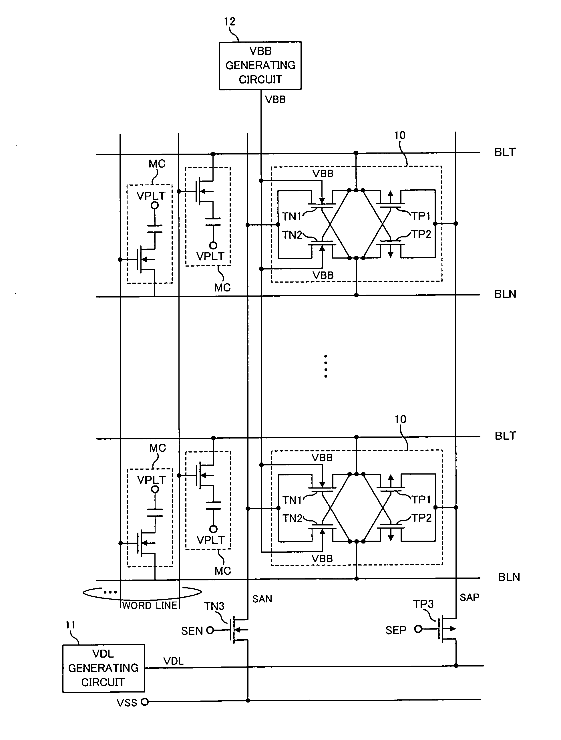
[0039]FIG. 1 is a diagram showing a primary configuration of DRAM of this embodiment. In FIG. 1, in an entire memory array of the DRAM in which a plurality of bit lines and a plurality of word lines are arranged in a matrix form, a circuit portion in which the same configuration is repeatedly arranged corresponding to a bit line pair BLT / BLN as a complementary pair is shown. In the circuit configuration of FIG. 1, in addition to a memory cell MC, a sense amplifier 10 and a VDL generating circuit 11 which are structural elements nearly common to FIG. 1, a VBB generation circuit 12 is also included.

[0040] On each bit line pair BLT / BLN, a sense amplifier 10 composed of a pair of NMOS transistors TN1 and TN2 (first NMOS transistors of the invention) and a pair of PMOS ...


PUM


Abstract

A semiconductor memory device comprising: a sense amplifier which includes a pair of first NMOS transistors and a pair of PMOS transistors connected to a bit line pair as a complementary pair; a back bias generating circuit which generates a back bias voltage to be applied to the first NMOS transistors in a state in which a predetermined current is flowing through a second NMOS transistor having approximately the same operating characteristic as that of the first NMOS transistors, and performs a feedback control in response to a threshold voltage of the second NMOS transistor; and control means which performs control in a sensing operation of the sense amplifier such that the pair of first NMOS transistors operates previously and after a lapse of a predetermined time the pair of first PMOS transistors operates.

Description

BACKGROUND OF THE INVENTION [0001] 1. Field of the Invention [0002] This invention relates to a semiconductor memory device having sense amplifiers for amplifying data held in a memory cell array. Particularly, this invention relates to a semiconductor memory device which employs N channel preceding sensing method for controlling operation of the sense amplifiers. [0003] 2. Related Art [0004] In general DRAM, a configuration is employed in which minute potential of a memory cell is read out and amplified by a sense amplifier disposed corresponding to a bit line pair as a complementary pair. FIG. 7 is a diagram showing a circuit configuration of a primary part of a conventional DRAM. In the circuit configuration of FIG. 7, a plurality of bit line pairs BLT / BLN is arranged repeatedly, and a plurality of memory cells MC each formed at an intersection of bit line BLT or BLN and a word line, a plurality of sense amplifiers each connected between the bit lines BLT and BLN and a VDL genera...

Claims


Application Information

Patent Timeline
Patent Type & Authority Applications(United States)
IPC IPC(8): G11C7/00
CPCG11C5/146G11C7/065G11C2207/065G11C11/4091G11C11/4074
Inventor TSUKADA, SHUICHI
Owner PS4 LUXCO SARL
Why Eureka
Try Eureka