A device for backside grinding of semiconductor wafers

A semiconductor and wafer technology, applied in the field of semiconductor wafer processing, can solve problems such as damage, increased cost, low efficiency, etc., to avoid waterproof and vulnerable to damage, improve efficiency, and facilitate liquid contact.

Active Publication Date: 2022-02-01
四川明泰微电子有限公司
View PDF18 Cites 0 Cited by
  • Summary
  • Abstract
  • Description
  • Claims
  • Application Information

AI Technical Summary

Problems solved by technology

Equipment with this structure requires special waterproof treatment for various electrical components, resulting in higher costs, and it is also difficult to avoid electrical components being corroded by liquids and causing damage
On the other hand, in the existing grinding equipment, the grinding disc is usually set coaxially with the wafer, and the wafer is polished by relative rotation. This structure can only process one wafer at a time, and the efficiency is low.

Method used


Image

  • A device for backside grinding of semiconductor wafers
  • A device for backside grinding of semiconductor wafers
  • A device for backside grinding of semiconductor wafers

Examples


Embodiment Construction

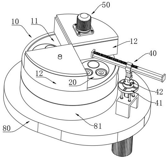
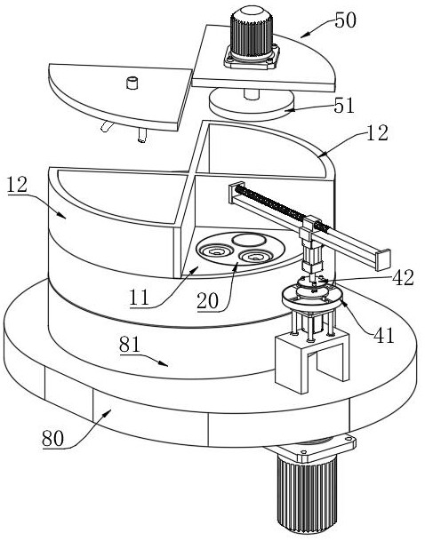
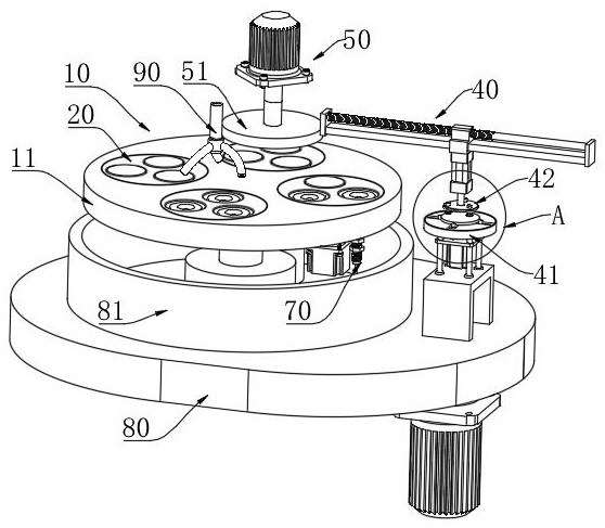
[0041] In order to make the purpose, technical solutions and advantages of the embodiments of the present invention clearer, the embodiments of the present invention will be described in detail below in conjunction with the accompanying drawings, but the embodiments described in the present invention are some of the embodiments of the present invention, not all of them .

[0042] It should be noted that like numerals and letters denote similar items in the following figures, therefore, once an item is defined in one figure, it does not require further definition and explanation in subsequent figures.

[0043] In describing the present invention, it should be noted that the terms "centre", "upper", "lower", "left", "right", "vertical", "horizontal", "inner", "outer" etc. indicate The orientation or positional relationship of the invention is based on the orientation or positional relationship shown in the drawings, or the orientation or positional relationship that is usually p...


PUM


Abstract

The present application provides a device for grinding the back of a semiconductor wafer, belonging to the field of wafer manufacturing, comprising: a running mechanism including a rotatable mounting plate, and the mounting plate has multiple mounting holes. The number of bearing discs is the same as that of the mounting holes, the bearing discs are rotatably arranged in the mounting holes, the bearing discs are provided with a plurality of sink holes along the circumference, and the bottom of the bearing discs is provided with a connecting part. The first driving part is located under the mounting plate, and the first driving part includes a driving pump, and a driving shaft is arranged to move along the axial direction of the rotating shaft of the driving pump. The feeding mechanism includes an alignment table and a suction cup. The grinding mechanism is arranged above the mounting plate corresponding to the first driving component, the grinding mechanism is provided with a grinding plate, and the positions corresponding to the grinding mechanism are provided above and below the mounting plate with sealing covers. It has high safety in use, is convenient for maintenance and inspection, and has high processing efficiency.

Description

technical field [0001] The invention belongs to the technical field of semiconductor wafer processing, and in particular relates to a device for grinding the back of a semiconductor wafer. Background technique [0002] The wafers used for the production of semiconductor devices mainly include crystal molding, shaping, slicing, and grinding. Semiconductor manufacturers need to thin the wafers provided upstream before manufacturing to meet the thickness required for semiconductor product design. At present, the wafers are mainly thinned by grinding. [0003] When polishing, it is necessary to spray the polishing liquid on the wafer. The liquid is not only used to wash and clean the wafer, but also contains additives in the polishing liquid to protect the chemical stability of the wafer. In the existing grinding device, various mechanisms are generally arranged in a sealed box, including various components driven by electricity, such as a motor that drives the rotation of the ...

Claims


Application Information

Patent Timeline
Patent Type & Authority Patents(China)
IPC IPC(8): B24B7/22B24B41/06B24B47/12B24B41/00
CPCB24B7/228B24B41/068B24B47/12B24B41/005
Inventor 袁根鲜浩
Owner 四川明泰微电子有限公司
Why Eureka
Try Eureka