In-chip multi-power system management circuit and method

A system management and power system technology, which is applied in the field of multi-power system management circuits in chips, can solve problems such as abnormal operation of chips, achieve precise control of delay time, avoid malfunctions, and eliminate malfunctions of chips.

Active Publication Date: 2021-12-21
四川创安微电子有限公司
View PDF13 Cites 0 Cited by
  • Summary
  • Abstract
  • Description
  • Claims
  • Application Information

AI Technical Summary

Problems solved by technology

[0004] The technical problem to be solved by the present invention is that when the chip is powered on, the power-on process and power-off process of each power system may cause the chip to have abnormal actions

Method used


Image

  • In-chip multi-power system management circuit and method
  • In-chip multi-power system management circuit and method
  • In-chip multi-power system management circuit and method

Examples


Embodiment 1

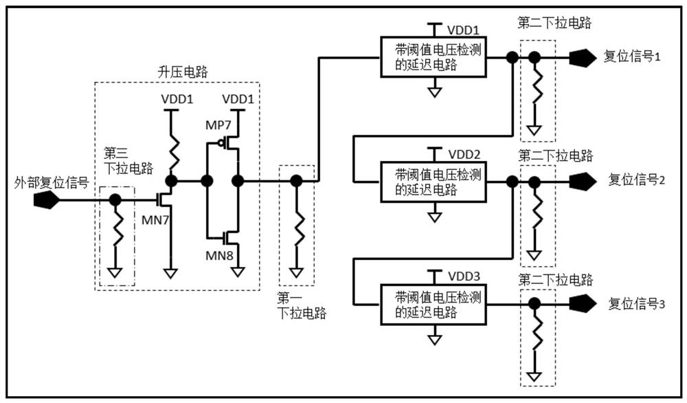
[0062] Such as Figure 1 to Figure 5 As shown, the present invention has a multi-power supply system management circuit in a chip, such as figure 1 As shown, the multi-power system management circuit provided in this embodiment includes a boost circuit, a first pull-down circuit, and three delay circuits, and the three delay circuits include a first delay circuit, a second delay circuit, and a third delay circuit. circuit;

[0063] One end of the boost circuit is connected to an external reset signal, the other end of the boost circuit is connected to a first pull-down circuit, and the first pull-down circuit is connected to the input end of the first delay circuit, and the output of the first delay circuit terminal outputs reset signal 1; the output terminal of the first delay circuit is also connected to the second delay circuit, and the output terminal of the second delay circuit outputs reset signal 2; the output terminal of the third delay circuit outputs reset signal 3;...

Embodiment 2

[0097] The difference between this embodiment and Embodiment 1 is that this embodiment provides an on-chip multi-power system management method, which is applied to the on-chip multi-power system management circuit described in Embodiment 1, and the method includes the above Three stages: before power-on, power-on, and power-off;

[0098] In the pre-power-on stage, the method includes:

[0099] When the external reset signal is in a steady state or in an unsteady state, the voltage of the external reset signal is fixed at a low potential of 0V through the third pull-down circuit, and the booster circuit does not work at this time;

[0100] The pull-down circuit can be implemented in various ways such as setting a resistor structure and setting a MOS tube.

[0101] The function of the pull-down circuit is to fix the voltage of the external reset signal at a low potential through the pull-down circuit, so as to prevent the chip from malfunctioning (that is, causing the chip to ...


PUM


Abstract

The invention discloses an in-chip multi-power system management circuit and method. The in-chip multi-power system management circuit comprises a booster circuit, a first pull-down circuit and a plurality of delay circuits, one end of the booster circuit is connected with an external reset signal, the other end of the booster circuit is connected with the first pull-down circuit, the first pull-down circuit is connected with the input end of the first delay circuit, and the output end of the first delay circuit outputs a reset signal 1; the output end of the first delay circuit is also connected with a second delay circuit, and the output end of the second delay circuit outputs a reset signal 2; ..., the output end of the (N-1) th delay circuit is also connected with the Nth delay circuit, and the output end of the Nth delay circuit outputs a reset signal N; each reset signal is led out to each functional unit in the chip; each delay circuit is correspondingly connected to a corresponding power supply system VDD; according to the multi-power-supply system management circuit, the reset state of the chip is sequentially relieved after each power supply system is powered on, and the chip enters the reset state in time when the power supply system is powered off.

Description

technical field [0001] The invention relates to the technical field of chip internal power supply management, in particular to a circuit and method for managing multiple power supply systems in a chip. Background technique [0002] In the process of external power supplying power to the chip, the common way is to divide the voltage through a voltage divider and supply it to each functional unit inside the chip. Each functional unit corresponds to a power system, so there are several power systems inside the chip. Due to a certain delay in the transmission process, there is a certain order in which the voltages detected by each power supply system exist. This results in that the functional unit that detects the voltage first is powered on first, and the functional unit that detects the voltage later is powered on instead of being powered on in the required order. [0003] In short, when the chip is powered on, the power-on process of each power supply system and the power-of...

Claims


Application Information

Patent Timeline
Patent Type & Authority Applications(China)
IPC IPC(8): G05F1/56
CPCG05F1/561
Inventor 不公告发明人
Owner 四川创安微电子有限公司
Why Eureka
Try Eureka