

Image projection device and vehicle lamp
An image projection and pattern technology, applied in projection devices, optics, instruments, etc., can solve the problems of reducing the wiring pattern on the circuit board, increasing the number of electrostatic protection elements 3, and reducing the miniaturization of the circuit board. the effect of
- Summary
- Abstract
- Description
- Claims
- Application Information
AI Technical Summary
Problems solved by technology
Method used
Image

Examples
no. 1 approach
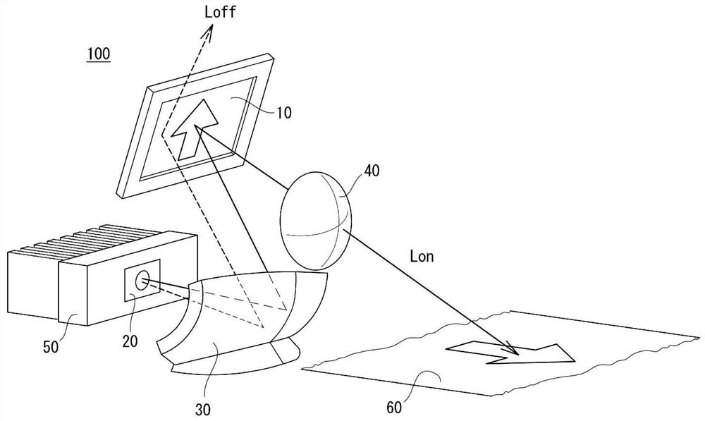
[0063] Hereinafter, embodiments of the present invention will be described in detail with reference to the drawings. The same or equivalent components, members, and processes shown in the drawings are assigned the same reference numerals, and redundant descriptions are appropriately omitted. figure 1 It is a schematic perspective view showing a configuration example of the vehicle lamp 100 according to the present embodiment. figure 1 The illustrated vehicle lamp 100 includes an image projection device 10 , a light source unit 20 , a reflector 30 , a projection lens 40 , and a heat sink 50 , and projects an image onto a projection surface 60 .
[0064]The image projection device 10 is a device that controls the reflection direction of in-plane light based on ON information and OFF information included in projected image information, and reflects light irradiated from the light source unit 20 as projection light Lon and shielding light Loff. The projection light Lon is irrad...
no. 2 approach
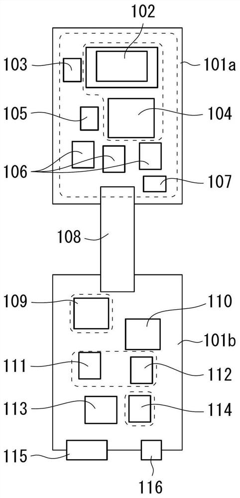
[0119] Next, use Figure 8 A second embodiment of the present invention will be described. Explanation of content overlapping with the first embodiment will be omitted. Figure 8 is a diagram showing the image projection device 10 of the present embodiment, Figure 8 (a) is a partially enlarged photograph showing a state where the mirror mounting substrate 101a and the power supply mounting substrate 101b are connected by a flexible cable 108, Figure 8 (b) is Figure 8 Partial enlarged view around the electrostatic protection element 122 in (a).
[0120] exist Figure 8 In the example shown in (a), the flexible cable 108 includes 39 single-ended wirings 108b and 108d, and 30 signal wiring patterns 121b and 121d are formed on the mirror mounting substrate 101a and the power supply mounting substrate 101b, respectively. Used as ESD protection element 122 Figure 7 In the shown element, since the electrostatic protection elements 122 are mounted on each of the four wiring ...
PUM
| Property | Measurement | Unit |
|---|---|---|
| Characteristic impedance | aaaaa | aaaaa |
| Characteristic impedance | aaaaa | aaaaa |
Abstract
Description
Claims
Application Information