Three-dimensional memory and manufacturing method thereof

A manufacturing method and memory technology, which can be used in semiconductor/solid-state device manufacturing, electric solid-state devices, semiconductor devices, etc., and can solve the problems of cumbersome processes and repeated steps.

Pending Publication Date: 2022-01-28
YANGTZE MEMORY TECH CO LTD
View PDF0 Cites 0 Cited by
  • Summary
  • Abstract
  • Description
  • Claims
  • Application Information

AI Technical Summary

Problems solved by technology

Two photolithography processes require two exposures, the process is cumbersome and the steps are repeated

Method used


Image

  • Three-dimensional memory and manufacturing method thereof
  • Three-dimensional memory and manufacturing method thereof
  • Three-dimensional memory and manufacturing method thereof

Examples


Embodiment Construction

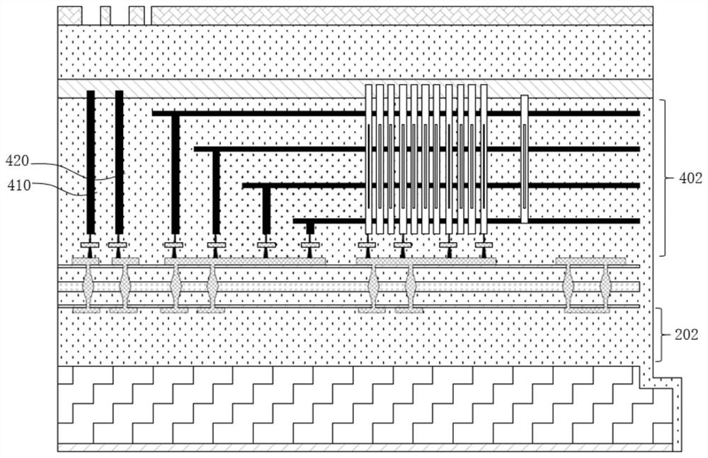
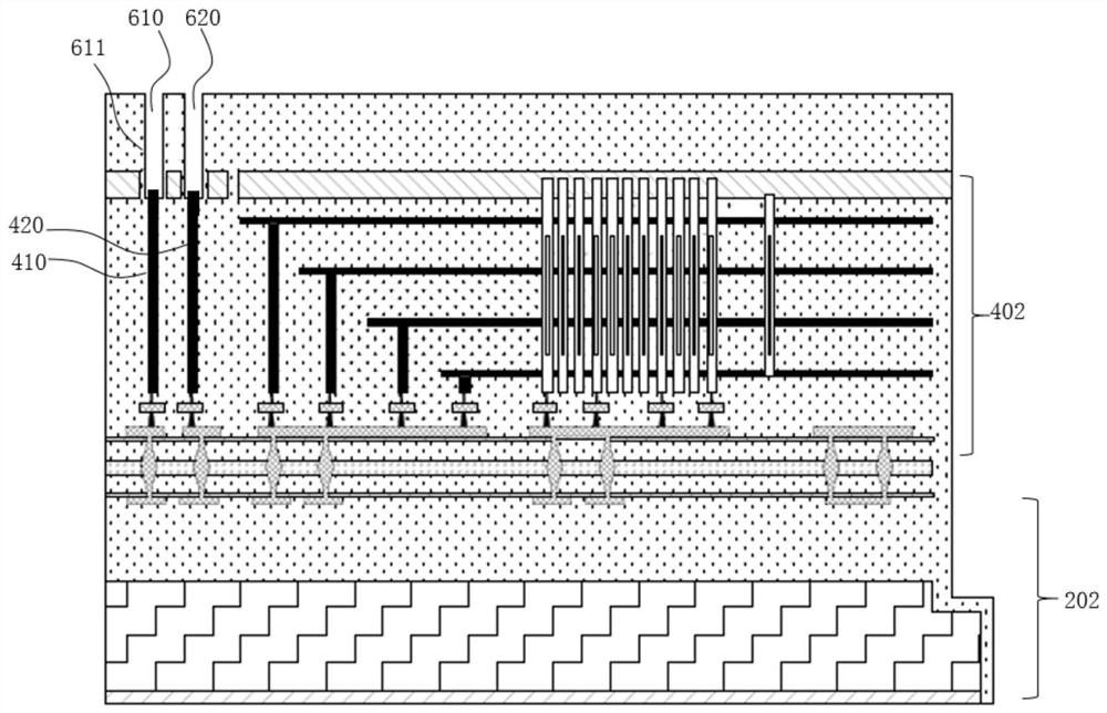
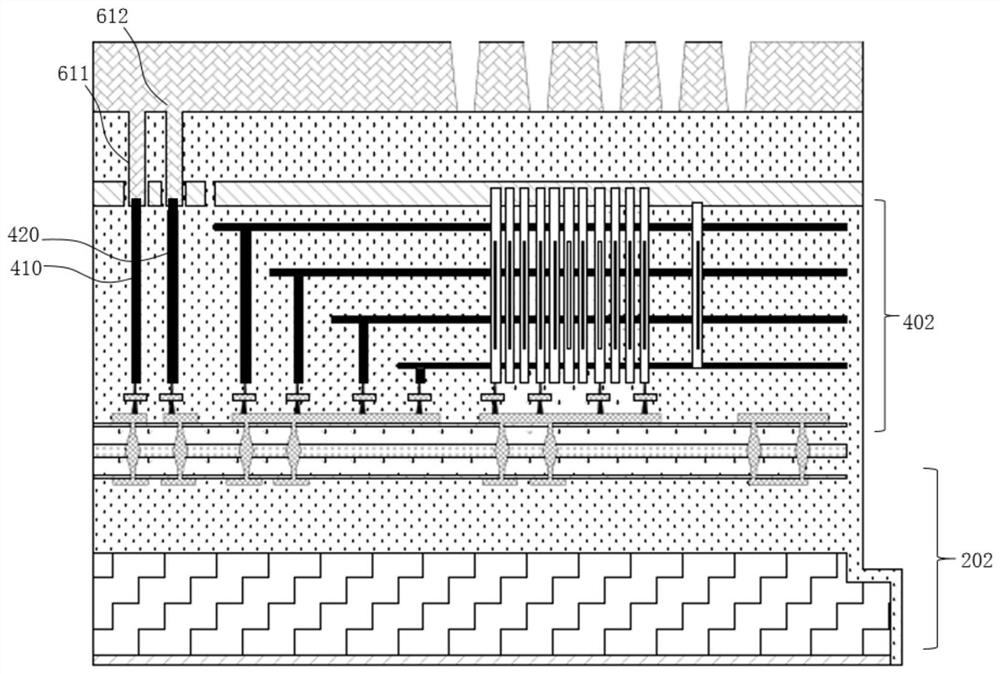
[0034] For a better understanding of the application, various aspects of the application will be described in more detail with reference to the accompanying drawings. It should be understood that these detailed descriptions are descriptions of exemplary embodiments of the application only, and are not intended to limit the scope of the application in any way. Throughout the specification, the same reference numerals refer to the same elements.

[0035] Note that references in the specification to "one embodiment," "an embodiment," "example embodiments," "some embodiments," etc. indicate that the described embodiments may include a particular feature, structure, or characteristic, but that each embodiment The specific feature, structure or characteristic may not necessarily be included. Moreover, these phrases are not necessarily referring to the same embodiment. In addition, when a particular feature, structure or characteristic is described in conjunction with an embodiment...


PUM

PropertyMeasurementUnit
transmittivityaaaaaaaaaa

Abstract

The invention provides a manufacturing method of a three-dimensional memory. The method comprises the steps: forming a mask layer on an insulating layer, wherein the mask layer comprises a first opening and a second opening, the first opening penetrates through the mask layer, and the bottom of the second opening is provided with the mask layer with a preset thickness; executing first etching which has a first etching selection ratio for the insulating layer and the mask layer with the preset thickness, etching the insulating layer to the bottom through the first opening, etching the mask layer through the second opening, and exposing at least part of the insulating layer; and executing second etching which has a second etching selection ratio for the semiconductor layer and the insulating layer, etching the semiconductor layer through the first opening and form a first contact hole penetrating through the insulating layer and the semiconductor layer, and simultaneously etching the insulating layer through the second opening and form a second contact hole exposing at least part of the semiconductor layer. A first through contact, a second through contact and an isolation structure can be formed at the same time, and the manufacturing process is simplified.

Description

technical field [0001] This application relates to the field of semiconductor technology. Specifically, the present application relates to a three-dimensional memory and a manufacturing method thereof. Background technique [0002] In the manufacturing process of the three-dimensional memory, on the one hand, in order to avoid leakage current and parasitic capacitance between the source contact and the word line formed on the front side of the storage stack structure, the source contact and the storage stack structure are usually arranged on polysilicon, for example The opposite side of the layer; on the other hand, it is necessary to form a through silicon contact (Through silicon contact, TSC) from the same side of the polysilicon layer as the source contact to transmit electrical signals with the external circuit. [0003] When forming the above-mentioned source contact and TSC, in some technologies, an opening corresponding to the TSC may be formed through a photolithog...

Claims


Application Information

Patent Timeline
Patent Type & Authority Applications(China)
IPC IPC(8): H01L21/768H01L23/538H01L27/11521H01L27/11551H01L27/11568H01L27/11578
CPCH01L21/76897H01L23/5386H10B41/20H10B43/30H10B43/20H10B41/30
Inventor 王溢欢
Owner YANGTZE MEMORY TECH CO LTD
Why Eureka
Try Eureka