Method for preparing ag nanowire array electrodes by magnetron sputtering-mask-assisted deposition

A technology of nanowire array and magnetron sputtering, which is applied in the direction of sputtering coating, manufacturing/processing of thermoelectric devices, ion implantation plating, etc., can solve the problem of not using mask-assisted deposition of Ag nanowire array to introduce devices, nano Linear performance is average, it is difficult to form large-scale production, etc., to achieve significant practical value and economic benefits, the production environment conditions are relaxed, and it is easy to achieve large-scale production.

Inactive Publication Date: 2017-05-17
TIANJIN UNIV OF SCI & TECH
View PDF5 Cites 0 Cited by
  • Summary
  • Abstract
  • Description
  • Claims
  • Application Information

AI Technical Summary

Problems solved by technology

[0004] The previous results revealed the synthesis of Ag nanowires. Because the nanowires prepared by chemical methods have many defects or need to remove the hard template, the performance of the nanowires is average, and it is difficult to form a large-scale production. It is also very difficult to introduce it into the device as a Electrode application; however, this is an innovative challenge, because the simple magnetron sputtering method to assemble Ag nanowire array structure films has not been reported, and there is no patent for using mask-assisted deposition of Ag nanowire arrays to introduce devices as electrodes with literature

Method used


Image

  • Method for preparing ag nanowire array electrodes by magnetron sputtering-mask-assisted deposition
  • Method for preparing ag nanowire array electrodes by magnetron sputtering-mask-assisted deposition
  • Method for preparing ag nanowire array electrodes by magnetron sputtering-mask-assisted deposition

Examples


Embodiment 1

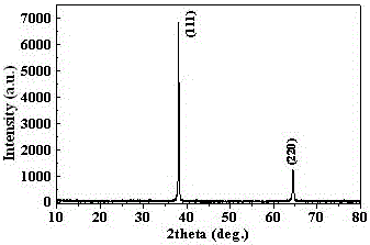
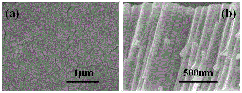
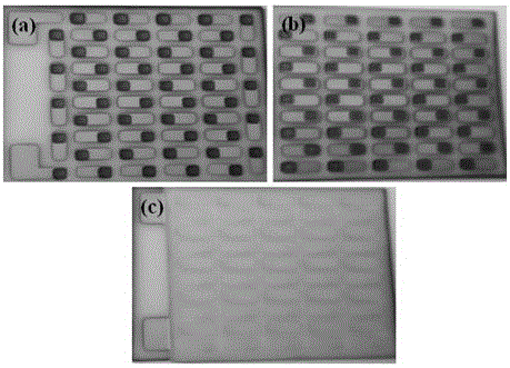
[0045] Fabrication of Ag nanowire arrays and 50 pairs of Ag nanowire array electrodes by magnetron sputtering-mask assisted deposition on AlN substrates p-n Device:

[0046] (1) The substrate was ultrasonically cleaned in acetone, absolute ethanol and deionized water for 10 minutes, then taken out, dried with high-purity nitrogen, and quickly placed in a sputtering vacuum chamber;

[0047] (2) Put the Ag target with a mass percentage purity of 99.99% into the magnetron sputtering vacuum chamber, adjust the distance between the substrate and the sputtering target source = 4, and start vacuuming;

[0048] (3) Vacuum up to 2.0×10 -4 Turn on the heating and temperature control power supply at Pa, set the heating temperature to 400°C, start to heat up the substrate, at the same time turn on the gas flow controller and the sputtering power supply to preheat, and turn on the sample stage to rotate (15 rpm);

[0049] (4) After the temperature rises to the predetermined temperature o...

Embodiment 2

[0060] Fabrication of Ag nanowire arrays and 50 pairs of Ag nanowire array electrodes by magnetron sputtering-mask-assisted deposition on AlN substrates p-n Device:

[0061] (1) The substrate was ultrasonically cleaned in acetone, absolute ethanol, and deionized water for 8 minutes, then taken out, dried with high-purity nitrogen, and quickly placed in a sputtering vacuum chamber;

[0062] (2) Put the Ag target with a mass percentage purity of 99.99% into the magnetron sputtering vacuum chamber, adjust the distance between the substrate and the sputtering target source = 3.5, and start vacuuming;

[0063] (3) Vacuum up to 3.0×10 -4 Turn on the heating and temperature control power supply at Pa, set the heating temperature to 350°C, start to heat up the substrate, and at the same time turn on the gas flow controller and the sputtering power supply to preheat, and turn on the sample stage to rotate (12 rpm);

[0064] (4) After the temperature rises to the predetermined tempera...

Embodiment 3

[0072] Preparation of columnar structure Ag film and 50 pairs of columnar structure Ag film electrodes on AlN substrate by magnetron sputtering-mask assisted deposition p-n Device:

[0073] (1) The substrate was ultrasonically cleaned in acetone, absolute ethanol, and deionized water for 8 minutes, then taken out, dried with high-purity nitrogen, and quickly placed in a sputtering vacuum chamber;

[0074] (2) Put the Ag target with a mass percentage purity of 99.99% into the magnetron sputtering vacuum chamber, adjust the distance between the substrate and the sputtering target source = 5, and start vacuuming;

[0075] (3) Vacuum up to 3.0×10 -4 Turn on the heating and temperature control power supply at Pa, set the heating temperature to 300°C, start to heat up the substrate, at the same time turn on the gas flow controller and the sputtering power supply to preheat, and turn on the sample stage to rotate (10 rpm);

[0076] (4) After the temperature rises to the predetermin...


PUM

PropertyMeasurementUnit
diameteraaaaaaaaaa
thicknessaaaaaaaaaa

Abstract

The invention relates to a method for preparing an Ag nanowire array electrode according to magnetron sputtering-masking assisted deposition, in particular to a method for preparing Ag films according to a magnetron sputtering and electrode masking assisted deposition technology. Metal electrode Ag target materials, which are connected, are deposited on an upper AlN substrate and a lower AlN substrate respectively; the sizes of both the upper AlN substrate and the lower AlN substrate are (1-40 mm)*(1-35 mm); then through alignment, p-Bi-Sb-Te film thermocouple arms and n-Bi-Te-Se film thermocouple arms are respectively deposited on prepared electrodes under the assistance of thermoelectric material masking; finally, several to thousands of p-Bi0.5Sb1.5Te3 film thermocouple arms and several to thousands of n-Bi2Se0.3Te2.7 film thermocouple arms, which are arranged on the upper AlN substrate and the lower AlN substrate respectively, form several to thousands of pairs of micro-devices adopting p-n structures through up-down bonding. Performance tests show that compared with the performance of a device with an electrode adopting the conventional structure, the performance of a device with the nanowire array electrode is improved significantly. Therefore, introduction of the Ag nanowire array electrode is an effective way to improve the performance of a thermoelectric micro-device. The method is simple in manufacture process, simple and convenient to operate, low in requirements on production environment, and very remarkable in practical value and economic benefits.

Description

technical field [0001] The invention relates to a technical method for preparing silver (Ag) nanowire arrays by simple physical vapor deposition method (magnetron sputtering), and introducing Ag nanowire array electrodes into devices through mask-assisted deposition; that is, it involves a A method for preparing Ag nanowire array electrodes by magnetron sputtering-mask assisted deposition. Background technique [0002] At present, the thermoelectric conversion efficiency that thermoelectric cells can achieve is only 4% to 6%, and most of the heat energy is wasted. Due to the low conversion efficiency, existing thermoelectric devices cannot fully meet the cooling requirements of high-power devices with increasing integration. The power density of thermoelectric devices is inversely proportional to the feature size, so micro thermoelectric devices can solve this difficulty well. However, the contact resistance and thermal resistance between metal electrodes and semiconductor...

Claims


Application Information

Patent Timeline
Patent Type & Authority Patents(China)
IPC IPC(8): C23C14/35C23C14/04C23C14/18H01L35/34
Inventor 谭明郝延明刘建静原凤英焦永芳谢宁
Owner TIANJIN UNIV OF SCI & TECH
Why Eureka
Try Eureka