Supercharge Your Innovation With Domain-Expert AI Agents!

Manufacturing method of display panel and manufacturing method of spliced display screen

A technology for display panels and manufacturing methods, which is applied to electrical components, electrical solid devices, circuits, etc., and can solve problems such as connection failure of the front and back sides of the substrate, the area of ​​the circuit not conforming to the development trend of high resolution, and the disconnection of the side connections, etc.

Pending Publication Date: 2022-02-11
CHONGQING KONKA PHOTOELECTRIC TECH RES INST CO LTD
View PDF0 Cites 0 Cited by
  • Summary
  • Abstract
  • Description
  • Claims
  • Application Information

AI Technical Summary

Problems solved by technology

Among them, the punching solution does not conform to the development trend of high resolution because it will occupy the area of ​​the circuit. It is difficult to realize the bending process in the bonding area of ​​the backplane. The side connection of the substrate is the mainstream direction.
[0003] There are currently the following problems in the connection on the side of the substrate. First, the connection material and the side are not well adhered. Second, the side connection is disconnected, which leads to the failure of the connection between the front and back of the substrate.

Method used


Image

  • Manufacturing method of display panel and manufacturing method of spliced display screen
  • Manufacturing method of display panel and manufacturing method of spliced display screen
  • Manufacturing method of display panel and manufacturing method of spliced display screen

Examples


Embodiment Construction

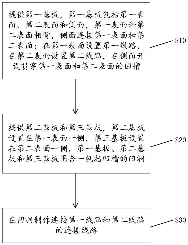
[0047]In order to facilitate the understanding of the present application, the present application will be described more fully below with reference to the relevant drawings. Preferred embodiments of the application are shown in the accompanying drawings. However, the present application can be embodied in many different forms and is not limited to the embodiments described herein. On the contrary, the purpose of providing these embodiments is to make the disclosure of the application more thorough and comprehensive.

[0048] Unless otherwise defined, all technical and scientific terms used herein have the same meaning as commonly understood by one of ordinary skill in the technical field to which this application belongs. The terminology used herein in the description of the application is only for the purpose of describing specific embodiments, and is not intended to limit the application.

[0049] A major application prospect of Micro-LED (Micro-light-emitting diode) disp...


PUM


Abstract

The invention relates to a manufacturing method of a spliced display screen and a display panel, and the method comprises the steps: providing a first substrate which comprises a first surface, a second surface and a side surface, the first surface and the second surface are opposite, and the side surface is connected with the first surface and the second surface; arranging a first circuit on the first surface, arranging a second circuit on the second surface, and forming a groove penetrating through the first surface and the second surface in the side face; providing a second base plate and a third base plate, wherein the second base plate is arranged on one side of the first surface, the third base plate is arranged on one side of the second surface, and the first base plate, the second base plate and the third base plate define a concave hole comprising a groove; and manufacturing a connecting line for connecting the first line and the second line in the concave hole. Through the arrangement, the adhesiveness of the connecting circuit and the first substrate can be improved; meanwhile, the groove has a protection effect on the connecting circuit, the probability of disconnection of the connecting circuit can be reduced, and the reliability of the display panel is improved.

Description

technical field [0001] The present application relates to the technical field of display panel manufacturing, and in particular to a method for manufacturing a display panel and a method for manufacturing a spliced ​​display screen. Background technique [0002] A major application prospect of Micro-LED (Micro-light-emitting diode) display technology is infinite splicing without size limitation. In order to achieve seamless splicing between display units, it is necessary to consider how to connect the wiring on the front and back surfaces of the substrate. Commonly used solutions in the industry are punching holes on the substrate, wiring on the side of the substrate, and bending the bonding area of ​​the front and back panels. and other programs. Among them, the punching solution does not conform to the high-resolution development trend because it will occupy the line area, and the bending process in the backplane bonding area is difficult to realize, and the side connecti...

Claims


Application Information

Patent Timeline
IPC IPC(8): H01L27/15H01L33/62
CPCH01L33/62H01L27/156
Inventor 潘飞刘政明
Owner CHONGQING KONKA PHOTOELECTRIC TECH RES INST CO LTD
Features
  • R&D
  • Intellectual Property
  • Life Sciences
  • Materials
  • Tech Scout
  • Unparalleled Data Quality
  • Higher Quality Content
  • 60% Fewer Hallucinations
Learn More