Display substrate, manufacturing method thereof and display device

A technology of display substrate and substrate substrate, which is applied to instruments, semiconductor devices, computing, etc., can solve the problems affecting the touch effect and display effect of the display substrate, and achieve the effect of avoiding the impact, ensuring the touch effect, and ensuring the display effect.

Pending Publication Date: 2022-04-15
BOE TECH GRP CO LTD +1
View PDF0 Cites 0 Cited by
  • Summary
  • Abstract
  • Description
  • Claims
  • Application Information

AI Technical Summary

Problems solved by technology

Since the display substrate usually includes an integrated gate drive (gate on array, GOA) circuit, the display signals transmitted in the display lines such as the input lines of the GOA circuit and the ou

Method used


Image

  • Display substrate, manufacturing method thereof and display device
  • Display substrate, manufacturing method thereof and display device
  • Display substrate, manufacturing method thereof and display device

Examples


Example Embodiment

[0047] In order to make the present application, the present application will be further described in connection with the accompanying drawings, which will be described in connection with the accompanying drawings. Based on the embodiments in the present application, one of ordinary skill in the art does not have all other embodiments obtained by creative labor, all of the present application protected.

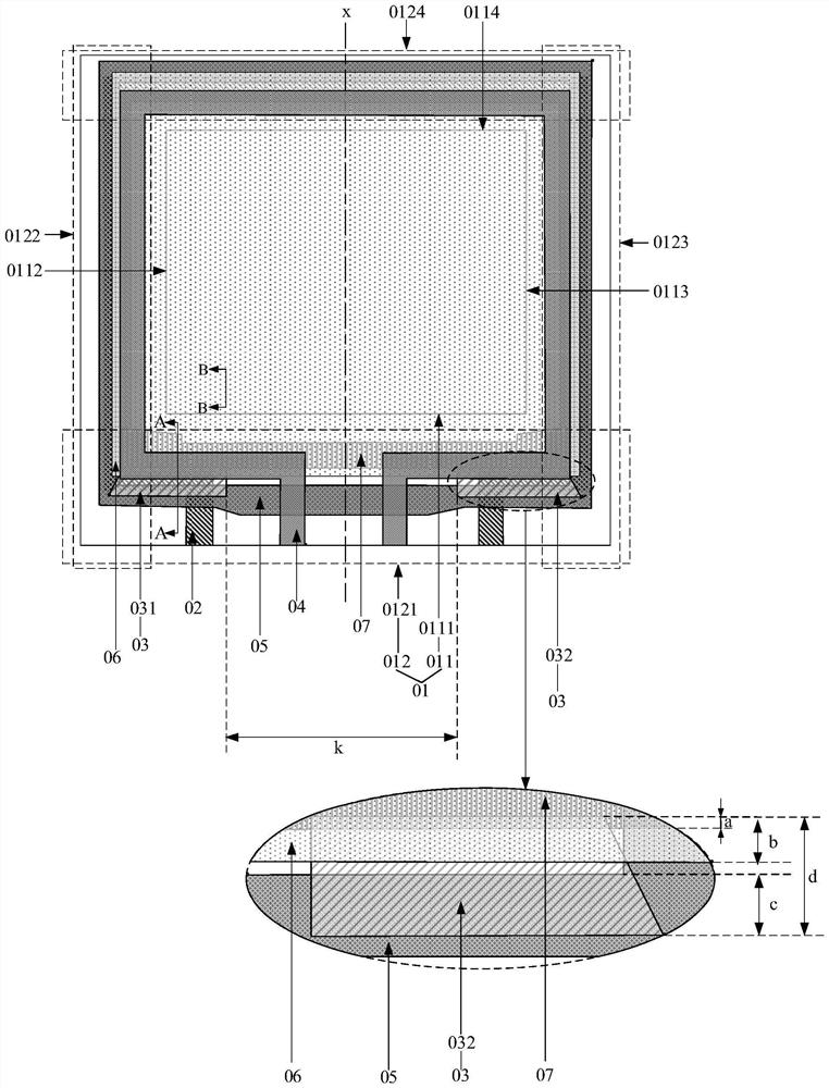
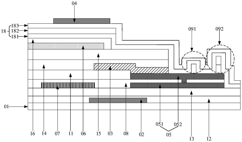
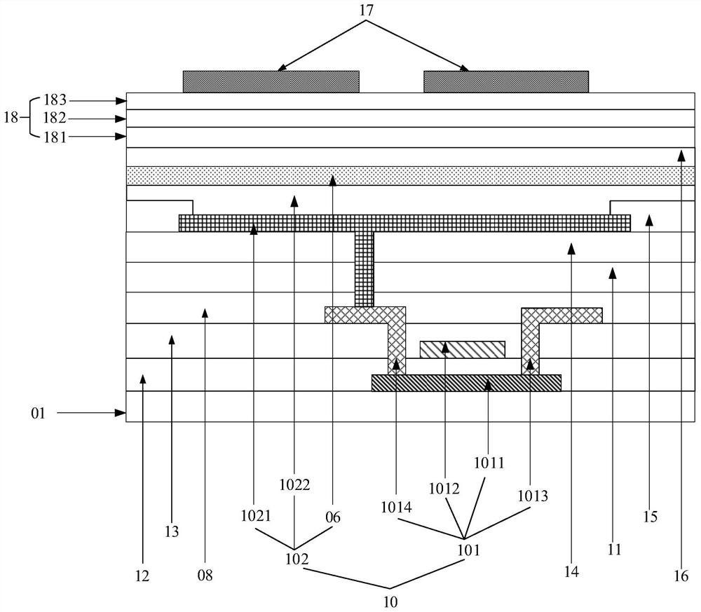
[0048] With the development of display technology, the display device begins to develop in a narrow border, a comprehensive screen, and the FMLOC technology came into being. Fmloc technology is a technique for making a touch structure on a package structure of the display substrate to integrate touch functions in the display substrate. The touch structure can include a touch electrode and a touch trace, and the touch trace is used to provide a touch signal to the touch electrode. The touch trace is also referred to as an Fmloc signal line, and the touch signal is also referred to...


PUM


Abstract

The invention discloses a display substrate, a manufacturing method thereof and a display device, and belongs to the technical field of display. The display substrate comprises a substrate body, a display wire, a shielding structure and a touch wire. The substrate comprises a display area and a peripheral area at least partially surrounding the display area. The display wire is located in the peripheral area and at least partially surrounds the display area. The shielding structure is located on the side, away from the substrate, of the display wire. The touch wires are located on the sides, away from the substrate, of the shielding structures. Orthographic projections of the display wire, the shielding structure and the touch wire on the substrate are at least partially overlapped. According to the invention, mutual interference between the display signal in the display wire and the touch signal in the touch wire can be shielded.

Description

technical field [0001] The present application relates to the field of display technology, in particular to a display substrate, a manufacturing method thereof, and a display device. Background technique [0002] The flexible multi-layer structure (Flexible Multi-Layer On Cell, FMLOC) technology refers to the technology of manufacturing a touch control structure on the packaging structure of the display substrate. The touch structure generally includes touch electrodes and touch wiring, and the touch wiring is used to provide touch signals to the touch electrodes. Since the display substrate usually includes an integrated gate drive (gate on array, GOA) circuit, the display signals transmitted in the display lines such as the input lines of the GOA circuit and the output lines of the GOA circuit are easily related to the signals transmitted in the touch line. The touch signals interfere with each other, affecting the touch effect and display effect of the display substrate....

Claims


Application Information

Patent Timeline
IPC IPC(8): H01L27/32G06F3/041
Inventor 易宏谷泉泳
Owner BOE TECH GRP CO LTD
Why Eureka
Try Eureka