Miniature LED chip, preparation method thereof and eutectic structure comprising miniature LED chip

A LED chip, miniature technology, applied in the direction of semiconductor devices, electrical components, circuits, etc., can solve the problems that the positive and negative electrodes are not on the same plane, the metal eutectic point of the negative electrode and the positive electrode are not on the same plane, and the eutectic effect cannot be achieved.

Pending Publication Date: 2022-05-13
FOSHAN ROUHAO ELECTRONICS CO LTD
View PDF0 Cites 0 Cited by
  • Summary
  • Abstract
  • Description
  • Claims
  • Application Information

AI Technical Summary

Problems solved by technology

[0009] This invention is to solve the problem that the positive and negative electrodes are not on the same plane when the Micro LED is eutectic. Since our LED structure adopts a common negative electrode structure, the LED negative electrode film layer and the LED positive electrode film layer are not on the same plane, which leads to the negative electrode and the LED positive electrode film layer. The problem that the positive metal eutectic point is not on the same plane, the eutectic effect cannot be achieved due to this problem during eutectic

Method used


Image

  • Miniature LED chip, preparation method thereof and eutectic structure comprising miniature LED chip

Examples


Embodiment 1

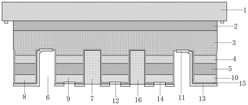
[0057] refer to figure 1 . The micro-LED chip of this embodiment includes a substrate 1, and a U-type gallium nitride layer 2, an N-type gallium nitride layer 3, a light-emitting layer 4, and a P-type gallium nitride layer extending outward from one side of the substrate 1 in sequence. Gallium nitride layer 5; the surface of the P-type gallium nitride layer 5 has a first groove 6 and a second groove 7 formed concavely and deep into the N-type gallium nitride layer 2, the first groove The periphery of 6 is a first protrusion 8, and the inner ring of the first groove 6 is a plurality of second protrusions 9, and the plurality of second protrusions 9 are separated by the second groove 7; the P-type nitride There is an insulating layer 10 on the gallium layer 5, the insulating layer 10 has a first opening 11 at the first groove 6, and the insulating layer 10 has a second opening 12 at the second protrusion 9; There is an N electrode layer 13 at the first opening 11, which is in ...


PUM


Abstract

The invention discloses a miniature LED chip, a preparation method thereof and a eutectic structure comprising the miniature LED chip, the surface of a P-type gallium nitride layer (5) of the miniature LED chip is provided with a first groove (6) and a second groove (7) which are formed in an inward concave mode and extend into an N-type gallium nitride layer (2), the periphery of the first groove (6) is provided with a first protrusion (8), the inner ring of the first groove (6) is provided with a plurality of second protrusions (9), and the second protrusions (9) are arranged on the periphery of the P-type gallium nitride layer (5). The plurality of second bulges (9) are spaced through second grooves (7); and the N electrode layer (13) on the first bulge (8) and the P electrode layer (14) on the second bulge (9) have the same horizontal height. According to the invention, the negative electrode of the LED is connected to the position on the same plane as the positive electrode, and the gap between the LED luminous points is filled with the anti-infrared material which can form a retaining wall between the LEDs, so that the LEDs are prevented from being deformed and even collapsed due to heating during eutectic, and the light of the LED luminous points on the two sides is also prevented from being blended.

Description

technical field [0001] The patent of the present invention belongs to the field of micro-LED technology, and specifically relates to a micro-LED chip, a preparation method thereof, and a eutectic structure containing it. Background technique [0002] Micro LED display technology refers to a display technology that uses self-luminous micron-scale LEDs as light-emitting pixel units and assembles them on the drive panel to form a high-density LED array. Due to the small size of the micro LED chip, high integration and self-illumination, compared with LCD and OLED in terms of display, it has greater brightness, resolution, contrast, energy consumption, service life, response speed and thermal stability. The advantages. [0003] Micro LED applications will expand from flat panel display to AR / VR / MR, space display, flexible transparent display, wearable / implantable optoelectronic devices, optical communication / optical interconnection, medical detection, smart car lights and many ...

Claims


Application Information

Patent Timeline
Patent Type & Authority Applications(China)
IPC IPC(8): H01L33/38H01L33/62H01L33/58H01L25/16H01L33/00
CPCH01L33/38H01L33/62H01L33/58H01L25/167H01L33/0075H01L33/0066H01L2933/0016H01L2933/0066H01L2933/0058
Inventor 林俊荣王宏吕河江
Owner FOSHAN ROUHAO ELECTRONICS CO LTD
Why Eureka
Try Eureka