Miniature LED chip detection structure and preparation method thereof

A technology for LED chips and detection structures, which is applied in semiconductor/solid-state device testing/measurement, electrical components, electric solid-state devices, etc. Crystal points are not on the same plane, etc., to achieve the effect of improving the quality of the eutectic

Pending Publication Date: 2022-04-19
FOSHAN ROUHAO ELECTRONICS CO LTD
View PDF0 Cites 0 Cited by
  • Summary
  • Abstract
  • Description
  • Claims
  • Application Information

AI Technical Summary

Problems solved by technology

[0010] This invention is to solve the problem that the positive and negative electrodes are not on the same plane when the Micro LED is eutectic. Since our LED structure adopts a common negative electrode structure, the LED negative electrode film layer and the LED positive electrode film layer are not on the same plane, which leads to the negative electrode and the LED positive electrode film layer. The problem that the positive metal eutectic point is not on the same plane, the eutectic effect cannot be achieved due to this problem during eutectic

Method used


Image

  • Miniature LED chip detection structure and preparation method thereof
  • Miniature LED chip detection structure and preparation method thereof

Examples


Embodiment 1

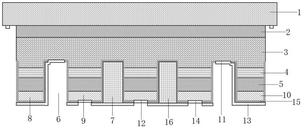
[0067] refer to figure 1 . The detection structure of the micro-LED chip in this embodiment is a common cathode and common anode structure, which includes a substrate 1, and a U-type gallium nitride layer 2 extending outward from one side of the substrate 1, and an N-type gallium nitride layer. Gallium layer 3, light-emitting layer 4 and P-type gallium nitride layer 5; the surface of the P-type gallium nitride layer 5 has a concave first groove 6 and a second groove formed deep into the N-type gallium nitride layer 2 Groove 7, the periphery of the first groove 6 is a first protrusion 8, the inner circle of the first groove 6 is a plurality of second protrusions 9, and a plurality of second protrusions 9 pass through the second concave grooves 7 intervals; the P-type gallium nitride layer 5 has an insulating layer 10, the insulating layer 10 has a first opening 11 at the first groove 6, and the insulating layer 10 has a first opening 11 at the second convex There is a second ...


PUM


Abstract

The invention discloses a miniature LED chip detection structure and a preparation method thereof, the surface of a P-type gallium nitride layer (5) of a miniature LED chip is provided with a first groove (6) and a second groove (7) which are formed in an inward concave mode and extend into an N-type gallium nitride layer (2), the periphery of the first groove (6) is provided with a first protrusion (8), the inner ring of the first groove (6) is provided with a plurality of second protrusions (9), and the second protrusions (9) are arranged on the periphery of the first groove (6). The plurality of second bulges (9) are spaced through second grooves (7); the N electrode layers (13) on the first protrusions (8) are connected together, and the P electrode layers (14) on the plurality of the second protrusions (9) are connected together. According to the invention, the common positive and negative structure of the LED chips is ensured, only different numbers of detection probes need to be arranged on the positive and negative electrodes of the LED according to the size of the module during detection, and then the positive and negative electrodes of the LED are electrified, so that all qualified LED chips are lightened. And after the detection is completed, the positive electrode of each LED is separated through an etching process, so that the difficulty of LED detection is solved.

Description

technical field [0001] The patent of the invention belongs to the field of micro-LED technology, and specifically relates to a micro-LED chip detection structure and a preparation method thereof. Background technique [0002] Micro LED display technology refers to a display technology that uses self-luminous micron-scale LEDs as light-emitting pixel units and assembles them on the drive panel to form a high-density LED array. Due to the small size of the micro LED chip, high integration and self-illumination, compared with LCD and OLED in terms of display, it has greater brightness, resolution, contrast, energy consumption, service life, response speed and thermal stability. The advantages. [0003] Micro LED applications will expand from flat panel display to AR / VR / MR, space display, flexible transparent display, wearable / implantable optoelectronic devices, optical communication / optical interconnection, medical detection, smart car lights and many other fields. It is esti...

Claims


Application Information

Patent Timeline
Patent Type & Authority Applications(China)
IPC IPC(8): H01L33/38H01L33/62H01L33/58H01L25/16H01L33/00H01L23/544
CPCH01L33/38H01L33/62H01L33/58H01L25/167H01L33/0075H01L33/0066H01L22/32H01L2933/0016H01L2933/0066H01L2933/0058
Inventor 林俊荣王宏吕河江
Owner FOSHAN ROUHAO ELECTRONICS CO LTD
Why Eureka
Try Eureka