Delay circuit

A delay circuit and delay signal technology, applied in electrical components, pulse technology, pulse processing, etc., can solve the problems of increasing circuit complexity, unable to support high-precision timing analysis, etc., and achieve high-precision results

Pending Publication Date: 2022-06-03
SHANGHAI CAMBRICON INFORMATION TECH CO LTD
View PDF0 Cites 0 Cited by
  • Summary
  • Abstract
  • Description
  • Claims
  • Application Information

AI Technical Summary

Problems solved by technology

[0002] With the development of semiconductor technology, the chip manufacturing process has entered the nanometer level. Although the chip has more functions and higher performance, it also greatly increases the complexity of the circuit, especially the chip's process defects, material defects, and life. Process deviations such as defects and environmental changes such as voltage and temperature are becoming more and more sensitive, so some high-precision test circuits are needed to evaluate the impact on timing when process deviations occur
[0003] Some test circuits in the prior art will introduce delay differences between sequential circuits by connecting multiple digital delay circuits in series. At present, the commonly used delay circuits use control signal delay circuit conduction and loopback. Such delay circuits are used in different In the process environment, the delay that can generally be generated is only about a dozen picoseconds, which cannot support high-precision timing analysis

Method used


Image

  • Delay circuit
  • Delay circuit
  • Delay circuit

Examples


Embodiment Construction

[0016] The following will be combined with the accompanying drawings in the present disclosure embodiment, the technical solution in the present disclosure embodiment is clearly and completely described, obviously, the embodiment described is a part of the embodiment of the present disclosure, not all embodiments. Based on the embodiments in the present disclosure, all other embodiments obtained by those skilled in the art without doing creative labor are within the scope of the protection of the present disclosure.

[0017] It should be understood that the terms "first", "second", "third" and "fourth" in the claims, description and drawings of the present disclosure are used to distinguish different objects, rather than to describe a particular order. The terms "comprising" and "wearing" as used in the specification and claims of the present disclosure indicate the existence of the features, wholes, steps, operations, elements and / or components described, but do not exclude the...


PUM


Abstract

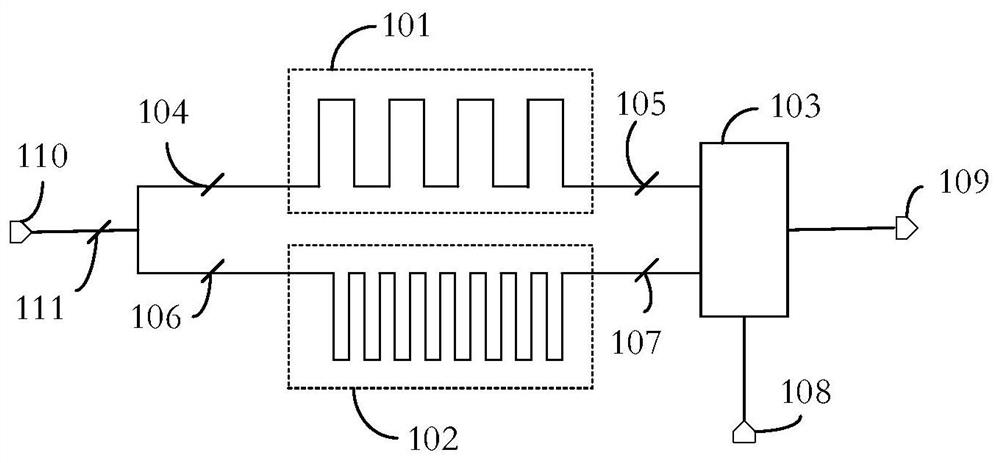
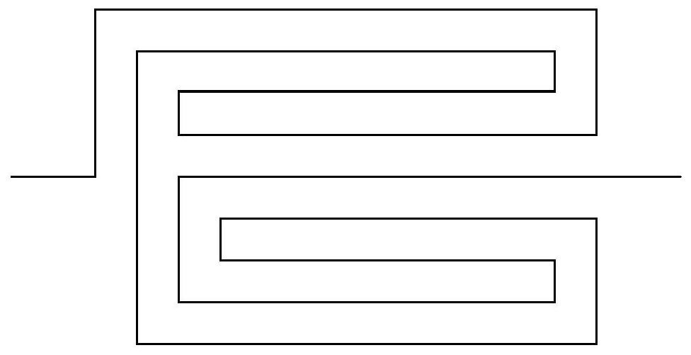
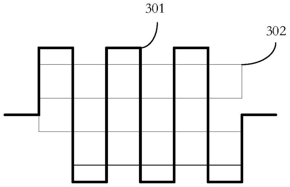
A delay circuit includes a first buffer, a second buffer, a wire, and a selector. The first buffer is configured to buffer an input signal to generate the first intermediate signal. The second buffer is used for buffering the input signal to generate the second intermediate signal. The winding is used for delaying the first intermediate signal to generate a delayed signal. The selector is configured to select the delayed signal or the second intermediate signal as an output signal. According to the invention, high-precision time sequence delay can be realized by adjusting the winding length.

Description

Technical field [0001] The present disclosure relates generally to the field of chip process testing. More specifically, the present disclosure relates to a high-precision digital delay circuit for testing chip process errors. Background [0002] With the development of semiconductor technology, the chip process has entered the nano level, although the chip has more functions and higher performance, but also greatly increased the complexity of the circuit, especially the chip to the process defects, material defects, life defects and other process deviations and voltage, temperature and other environmental changes are more and more sensitive, so the need for some high-precision test circuits to assess the impact on timing when process deviations occur. [0003] Some test circuits of the prior art will introduce the delay difference between the timing circuits by series a plurality of digital delay circuits, and the currently commonly used delay circuit is to use the control signa...

Claims


Application Information

Patent Timeline
Patent Type & Authority Applications(China)
IPC IPC(8): H03K5/00
CPCH03K5/00H03K2005/0015
Inventor 不公告发明人
Owner SHANGHAI CAMBRICON INFORMATION TECH CO LTD
Why Eureka
Try Eureka