
Semiconductor device

A technology of semiconductors and transistors, which is applied in the field of semiconductor devices and can solve problems such as wiring conflicts

Pending Publication Date: 2022-07-29
SOCIONEXT INC
View PDF5 Cites 0 Cited by
  • Summary
  • Abstract
  • Description
  • Claims
  • Application Information

AI Technical Summary

Problems solved by technology

[0009] However, in the case of using a metal wiring layer close to the semiconductor substrate to form a dummy power line wired between the power switch circuit and the circuit module, there is a possibility that the wiring formed using a metal wiring layer close to the semiconductor substrate and the dummy power supply line in the power switch circuit Line Conflict Concerns

Method used


Image

  • Semiconductor device
  • Semiconductor device
  • Semiconductor device

Examples


no. 1 approach

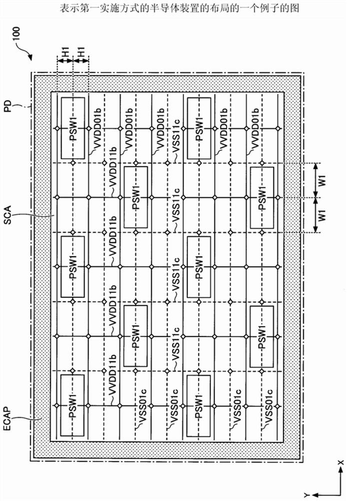
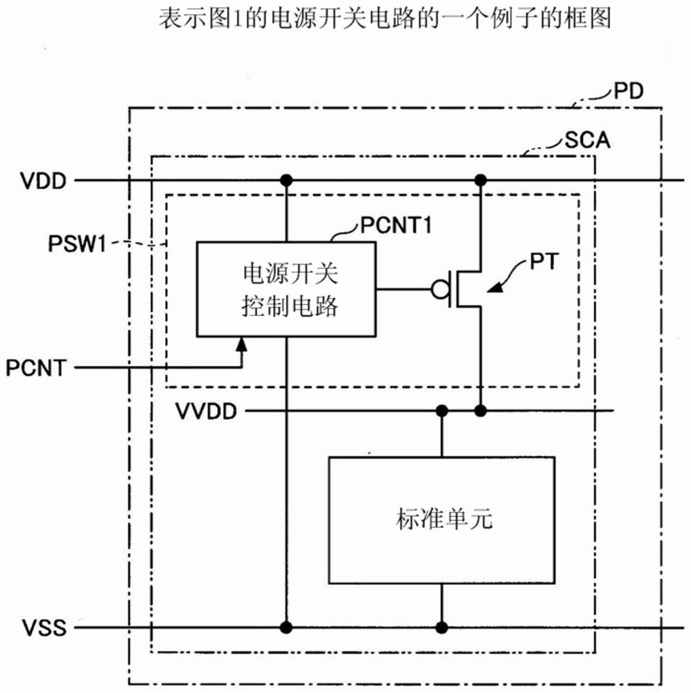
[0029] figure 1 An example of the layout of the semiconductor device in the first embodiment is shown. figure 1 The semiconductor device 100 shown has, for example, at least one power domain PD. A standard cell area SCA in which a plurality of standard cells (not shown) are arranged is provided in the power domain PD. Although not particularly limited, the transistor mounted on the semiconductor device 100 is a finFET. finFET in Figure 5 explained in. The standard cell area SCA is an example of a first area where logic circuits can be configured.

[0030] An end cap ECAP shown in a hatched pattern is arranged around the standard cell area SCA. The end cap ECAP has a dummy gate electrode or a dummy transistor not shown. In addition, in the standard cell area SCA, in figure 1 The longitudinal direction, that is, the Y direction, is alternately arranged with an interval H1. figure 1 The virtual power supply line VVDD01b and the ground line VSS01c extending in the lateral...

no. 2 approach

[0072] Figure 7 An example of the layout of the power switch circuit of the semiconductor device in the second embodiment is shown. right and image 3 The same elements are assigned the same reference numerals, and detailed descriptions are omitted. have Figure 7 The layout of the semiconductor device of the power switch circuit PSW1 shown is the same as figure 1 The layout of the semiconductor device 100 is the same. That is, having Figure 7 The semiconductor device of the illustrated power switch circuit PSW1 has a standard cell area SCA in which a plurality of standard cells are arranged in the power domain PD, and the power switch circuit PSW1 is arranged in the standard cell area SCA.

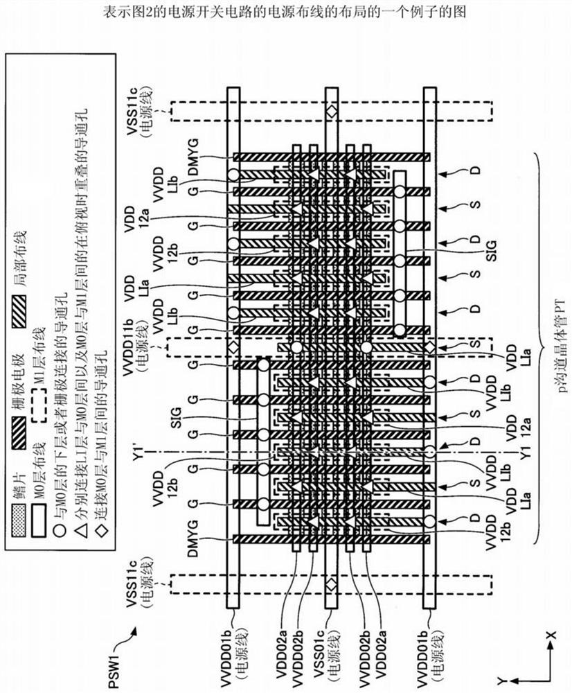
[0073] In this embodiment, the power supply line VVDD11b of the M1 layer arranged along the Y direction at the central portion in the X direction of the power supply switch circuit PSW1 is connected to the M0 layer wiring VVDD02b extending in the X direction through the via hole sh...

no. 3 approach

[0076] Figure 8 An example of the layout of the power switch circuit of the semiconductor device in the third embodiment is shown. right and image 3 as well as Figure 7 The same elements are assigned the same reference numerals, and detailed descriptions are omitted. have Figure 8 The layout of the semiconductor device of the power switch circuit PSW1 shown is the same as figure 1 The layout of the semiconductor device 100 is the same. That is, having Figure 8 The semiconductor device of the illustrated power switch circuit PSW1 has a standard cell area SCA in which a plurality of standard cells are arranged in the power domain PD, and the power switch circuit PSW1 is arranged in the standard cell area SCA.

[0077] In this embodiment, on the power switch circuit PSW1, in addition to the power supply line VVDD11b of the M1 layer extending in the Y direction, the power supply line VSS11c of the M1 layer extending in the Y direction is also wired on the p-channel tran...


PUM


Abstract

The invention provides a semiconductor device. When a power line such as a dummy power line is formed using a metal wiring layer close to a semiconductor substrate, collision between a first power line and wiring in a power switch circuit is avoided. The first and second power supply lines are formed in the first wiring layer and extend in a first direction in plan view. A third power supply line connected to the first power supply line and a fourth power supply line connected to the second power supply line, formed in the second wiring layer, and extending in the second direction in plan view; and a first power switch circuit having a transistor provided between the first power supply line and a fifth power supply line formed in the first wiring layer and overlapping with at least one of the third power supply line and the fourth power supply line, the first power switch circuit having a second power switch circuit formed in the second wiring layer so as not to overlap with the third power supply line and the fourth power supply line. A first wiring electrically connected to the source region of the transistor and the fifth power supply line; and a second wiring electrically connected to the drain region of the transistor and the third power supply line.

Description

technical field [0001] The present invention relates to semiconductor devices. Background technique [0002] In order to reduce the leakage current of the semiconductor device, there is known a method of providing a power switch circuit that is turned on when the circuit module operates between a power supply line and a virtual power supply line that is a power supply line of each of a plurality of circuit modules. For example, in order to improve the power supply capability of the power switch circuit, the size of the transistor used in the power switch circuit is designed to be larger than the size of the unit transistor used in the logic circuit in the circuit module. [0003] Patent Document 1: Specification of US Patent No. 10141336 [0004] Patent Document 2: Specification of US Patent Application Publication No. 2019 / 0244900 [0005] Patent Document 3: Specification of US Patent Application Publication No. 2019 / 0214377 [0006] Patent Document 4: Japanese Patent La...

Claims


Application Information

Patent Timeline
IPC IPC(8): H01L27/02H01L23/528
CPCH01L27/0207H01L23/528H01L23/5286H01L2027/11881H01L27/11807H01L23/5226H01L23/5283
Inventor 武野纮宜冈本淳日野寿雄
Owner SOCIONEXT INC
Learn More