Defect detection device for large-breadth silk screen

A defect detection and surface screen technology, which is applied in the direction of measuring devices, instruments, and final product manufacturing, can solve problems such as low efficiency, difficulty in identification, and insufficient accuracy

Pending Publication Date: 2022-08-09
武汉光目科技有限公司
View PDF0 Cites 2 Cited by
  • Summary
  • Abstract
  • Description
  • Claims
  • Application Information

AI Technical Summary

Problems solved by technology

[0003] In most of the existing wire mesh inspection processes, defects are often detected by manually observing the wire mesh with the naked eye. This traditional method is inefficient and requires a lot of time and labor costs.
In the past two years, some automatic screen inspection equipment has appeared, which detects screen defects through image acquisition equipment and machine vision algorithms. However, these screen inspection devices also need to spend a lot of time when facing large-format screen printing screens. time; and machine vision algorithms are affected by hardware such as light sources and cameras, there are still some defects that are difficult to identify, and the accuracy rate is not high enough

Method used


Image

  • Defect detection device for large-breadth silk screen
  • Defect detection device for large-breadth silk screen
  • Defect detection device for large-breadth silk screen

Examples


Embodiment Construction

[0035] In order to make the objectives, technical solutions and advantages of the present invention clearer, the present invention will be further described in detail below with reference to the accompanying drawings and embodiments. It should be understood that the specific embodiments described herein are only used to explain the present invention, but not to limit the present invention.

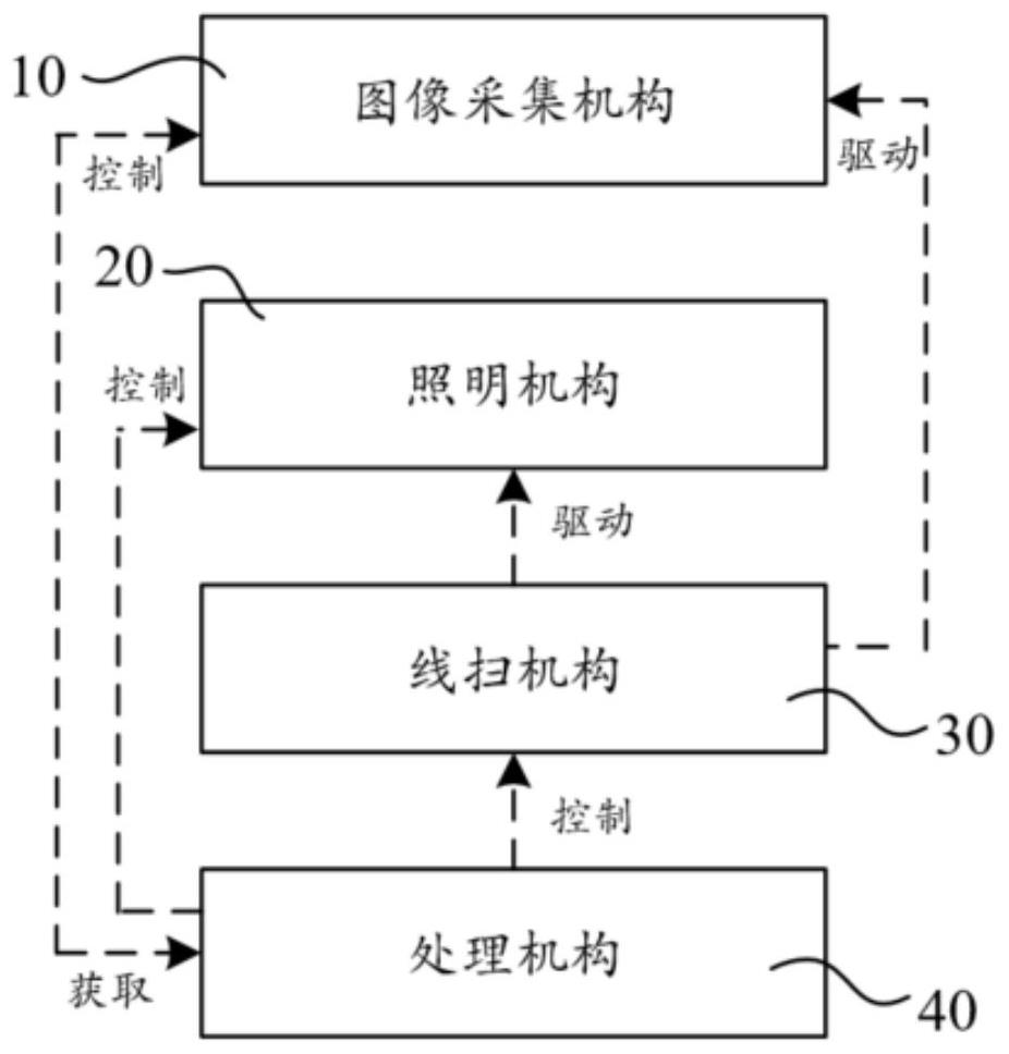
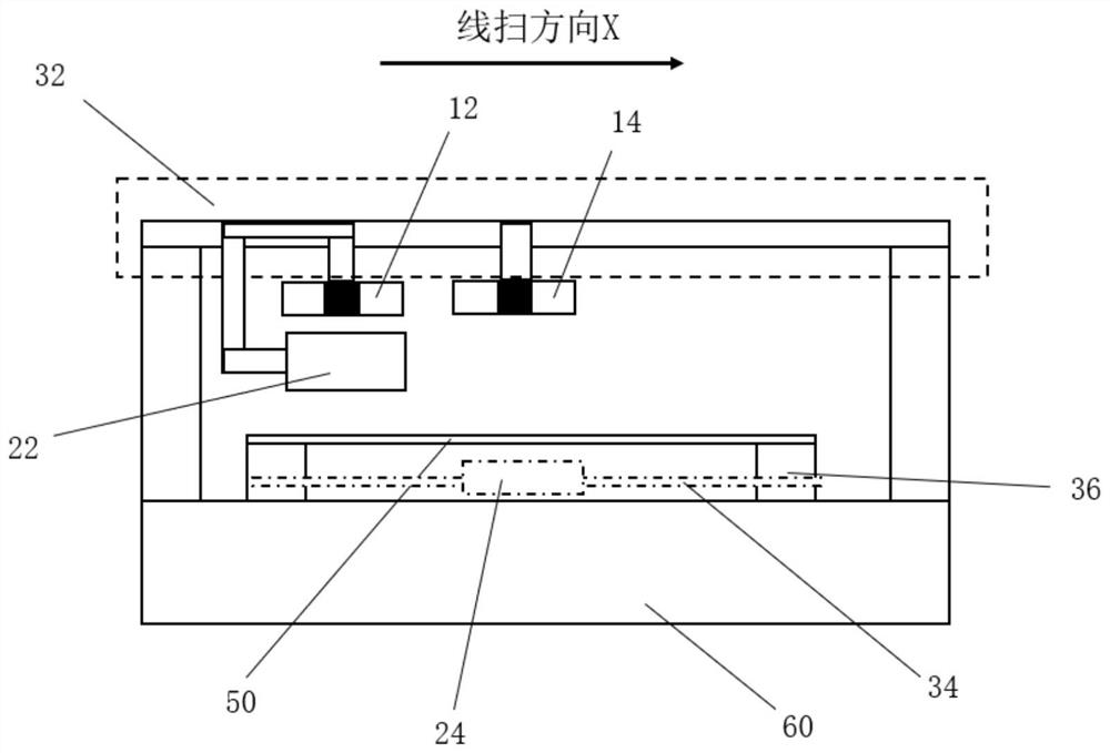
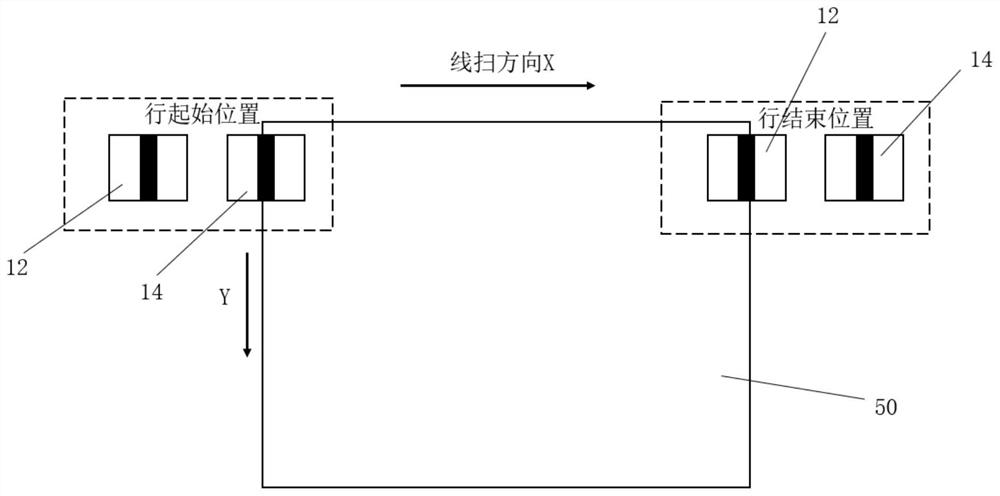
[0036] figure 1 It is a schematic structural diagram of a large-format wire mesh defect detection device provided by an embodiment of the present invention, such as figure 1 As shown, the present invention provides a large-format wire mesh defect detection device, including a support machine 60 and a clamping mechanism (not shown in the figure) arranged in the support machine 60, an image acquisition mechanism 10, and an illumination mechanism 20. , line sweeping mechanism 30 and processing mechanism 40 .

[0037] The clamping mechanism is used to place and fix the wire mesh 50 to be tes...


PUM


Abstract

The invention discloses a large-breadth silk screen defect detection device which comprises an image acquisition mechanism which comprises two CCD (Charge Coupled Device) linear array cameras arranged along the same X-axis position, the pixel arrangement direction of the CCD linear array cameras is parallel to the Y-axis, and the spacing distance between the two CCD linear array cameras is an integral multiple of the length of each pixel of the CCD cameras in an X-axis field of view; the lighting mechanism comprises an upper light source and a lower light source; the line scanning mechanism is used for simultaneously driving the upper light source and the two CCD line-scan digital cameras to move along the X axis, driving the lower light source to synchronously move along the X axis along with the second CCD line-scan digital camera, and driving the silk screen to be detected to move along the Y axis; and the processing mechanism is used for performing alignment cutting on the acquired row images correspondingly acquired by the two CCD linear array cameras, and performing defect detection on each row image correspondingly acquired by the two CCD linear array cameras after alignment cutting through a machine vision algorithm by adopting a double-light-source image joint detection algorithm. According to the invention, the image acquisition speed and the defect detection accuracy in silk screen defect detection can be effectively improved.

Description

technical field [0001] The invention belongs to the technical field of wire mesh detection, and more particularly relates to a large-format wire mesh defect detection device. Background technique [0002] With the introduction of the concept of Industry 4.0, the intelligentization of industrial production has increasingly become an important step in the process of industrial upgrading in my country. Among them, machine vision detection technology has been applied in more and more fields, significantly improving the efficiency of industrial production in various fields and saving a lot of costs. In the photovoltaic screen printing process, the integrity of the screen printing screen (referred to as the screen) affects the quality of the subsequent printed electrodes. Therefore, defect detection of the screen is an important step. [0003] In most of the existing wire mesh inspection processes, defects are often detected by manually observing the wire mesh with the naked eye....

Claims


Application Information

Patent Timeline
Patent Type & Authority Applications(China)
IPC IPC(8): G01N21/892G01N21/01
CPCG01N21/892G01N21/01G01N2021/8927G01N2021/8887Y02P70/50
Inventor 雷力于龙
Owner 武汉光目科技有限公司
Why Eureka
Try Eureka