Rear shallow groove isolating process

A process method, shallow trench isolation technology, applied in the direction of electrical components, semiconductor/solid-state device manufacturing, circuits, etc., can solve the problems of abnormal electrical performance of semiconductor components, reduce the electrical isolation effect of shallow trench isolation, and poor double ridges, etc. Achieve the effect of shortening production time and cost

Inactive Publication Date: 2004-12-15
MACRONIX INT CO LTD
View PDF0 Cites 0 Cited by
  • Summary
  • Abstract
  • Description
  • Claims
  • Application Information

AI Technical Summary

Problems solved by technology

When the gate oxide layer is subsequently formed, the gate oxide thinning phenomenon (gate oxide thinning) in the corner region 23 of the shallow trench is easy to occur, thereby reducing the electrical isolation effect of the shallow trench isolation, which in turn leads to abnormal electrical properties of the semiconductor element, such as The Id / Vg curve produces a bad double hump variation, reducing the reliability of the product;
[0009] 3). Existing shallow trench isolation methods require an additional corner rounding step; and
[0010] 4). The existing shallow trench isolation method uses the CMP method, which is easy to cause damage to the silicon substrate, and is prone to shallow dish effect

Method used


Image

  • Rear shallow groove isolating process
  • Rear shallow groove isolating process
  • Rear shallow groove isolating process

Examples


Embodiment Construction

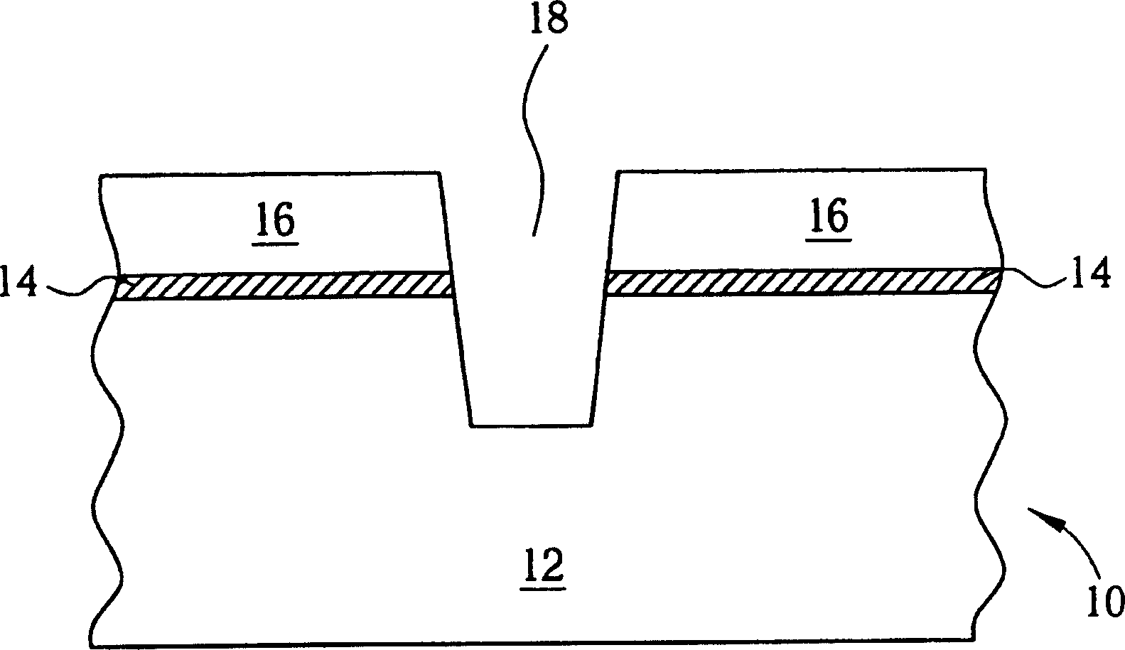
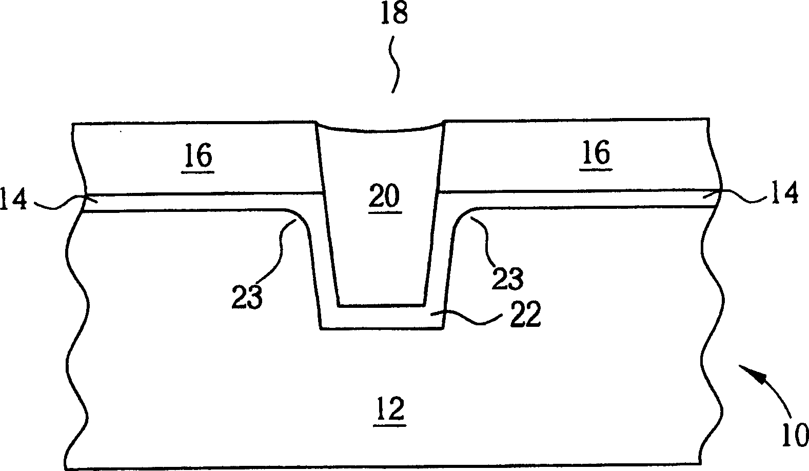
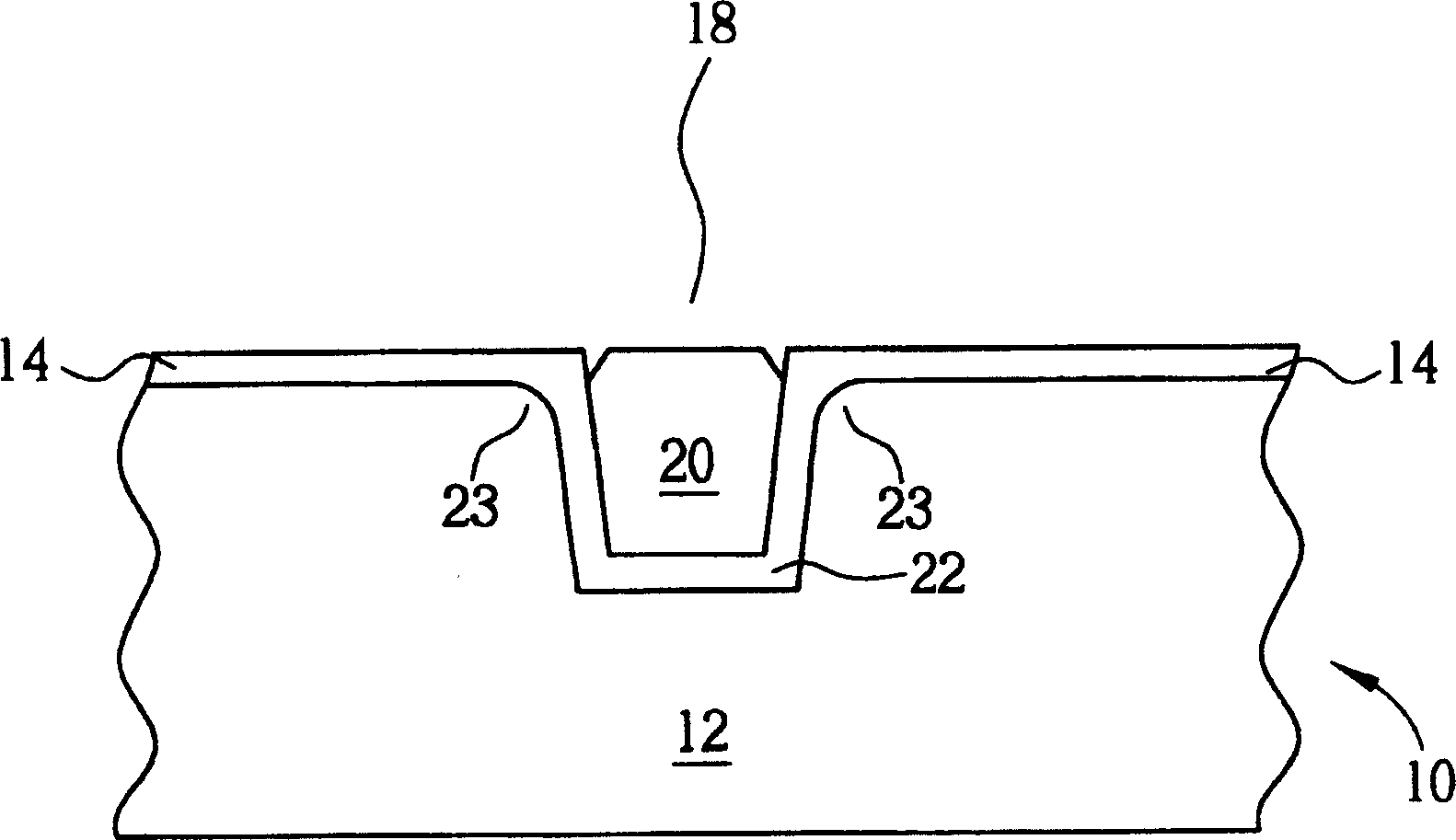
[0031] A post shallow trench isolation (post-STI) process method of the present invention is to fabricate semiconductor elements, such as gates and MOS transistors, on a substrate first, and then perform the shallow trench isolation process. The inventive method mainly has the following steps:

[0032] 1). Provide a substrate, the substrate has an upper surface;

[0033] 2). Carrying out a first ion implantation process to form a doped well region on the upper surface of the substrate;

[0034] 3). Forming an oxide layer on the upper surface of the substrate;

[0035] 4). Depositing a polysilicon layer on the oxide layer;

[0036] 5). Etching the polysilicon layer to form a gate in the doped well region;

[0037] 6). Performing a second ion implantation process to form a drain region and a source region on both sides of the gate in the doped well region;

[0038] 7). Forming a first dielectric layer on the substrate to cover the doped well region, the gate and regions other ...


PUM


Abstract

The invention provides a rear shallow groove isolating process. At first, an impure well region is formed at an upper surface of a substrate, and an oxide and a polycrystal silicon layer are orderly formed on the upper surface of the substrate. Subsequently, the polycrystal silicon layer is etched to form a gate in the impure well region, and a drain / source region is formed at two sides of the gate. Thereafter, a first dielectric layer is formed on the substrate to cover the impure well region, the gate and regions except for the impure well region, after that, a second dielectric layer having an approximate flat surface is formed to cover the first dielectric layer. Then a photoresist layer is formed on the second dielectric layer to cover the impure well region, the second dielectric layer, the first dielectric layer and the substrate at outside of the impure well region are eteched to configure a trench region. Finally, the photoresist layer is removed, a third dielectric layer is deposited to be filled in the trench region and cover the second dielectric layer.

Description

technical field [0001] The invention provides a post shallow trench isolation (post-STI) process method, which first forms components, and then forms an insulating trench region, and in particular relates to a post shallow trench that avoids recesses in the corner regions of the shallow trench Isolation process method. Background technique [0002] In the semiconductor process, in order to have a good isolation between the various electronic components on the chip to avoid short circuit caused by mutual interference between the components, localized oxidation isolation (LOCOS) or shallow trench isolation methods are generally used for isolation. with protection. Since the area of ​​the chip occupied by the field oxide produced in the LOCOS process is too large, and the formation process will be accompanied by the bird's beak phenomenon, the current semiconductor process with a line width below 0.25 μm is almost Both adopt the shallow trench isolatio...

Claims


Application Information

Patent Timeline
Patent Type & Authority Patents(China)
IPC IPC(8): H01L21/76
Inventor 曹铕张国华邱宏裕李俊鸿
Owner MACRONIX INT CO LTD
Why Eureka
Try Eureka