Shallow-channel insulation making process

A technology of shallow trenches and liner layers, applied in semiconductor/solid-state device manufacturing, electrical components, circuits, etc., can solve the problems of reduced product reliability, abnormal conductivity of semiconductor components, poor double-bumps, etc., to improve reliability. degree, enhance product competitiveness, and ensure the effect of electrical insulation effect

Inactive Publication Date: 2003-05-14
MACRONIX INT CO LTD
View PDF0 Cites 4 Cited by
  • Summary
  • Abstract
  • Description
  • Claims
  • Application Information

AI Technical Summary

Problems solved by technology

The high electric field effect of the shallow trench corner region 23 will cause carrier inversion in the shallow trench corner region to form a low initial voltage channel parallel to the main element, resulting in an increase in element leakage current, which is the secondary initial voltage neck knot (sub-threshold kink) phenomenon
In addition, the oxide layer depression 24 will make the shallow trench corner region 23 very susceptible to etching during the subsequent acid solution immersion cleaning process, which will reduce the electrical insulation effect of the shallow trench insulation, and further cause the conductivity of the semiconductor element to be abnormal. For example, the Id / Vg curve produces a bad double hump variation, which reduces the reliability of the product

Method used


Image

  • Shallow-channel insulation making process
  • Shallow-channel insulation making process
  • Shallow-channel insulation making process

Examples


Embodiment Construction

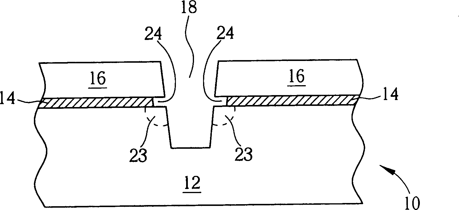
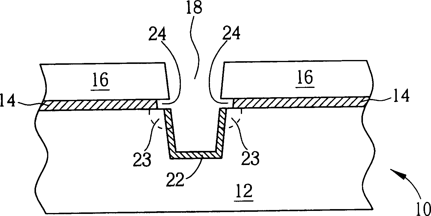
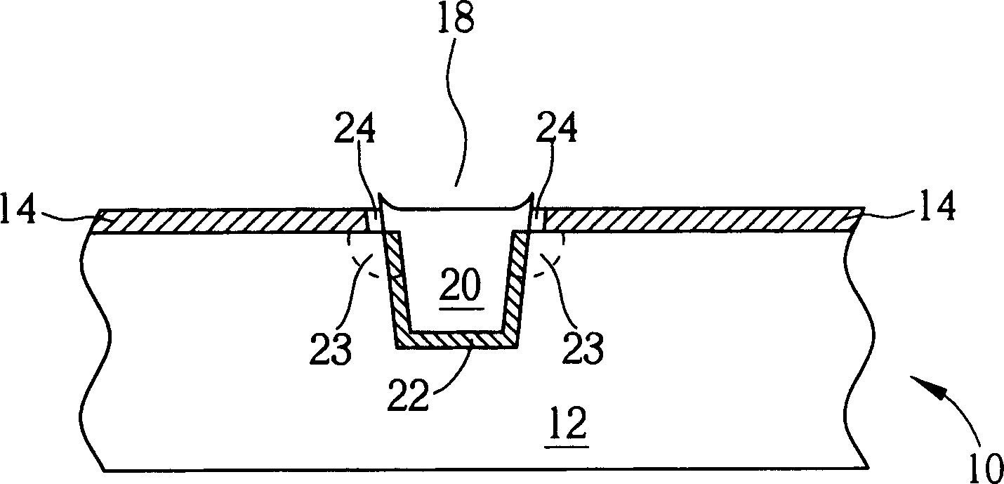
[0024] Please refer to Figure 4 to Figure 8 , Figure 4 to Figure 8 It is a schematic diagram of the shallow trench isolation process method of the present invention. Such as Figure 4 As shown, the semiconductor wafer 30 includes a silicon substrate 32 and a stacked mask layer 37 composed of a pad oxide layer 34 and a stopper layer 36 and having at least one opening 46 exposing a portion of the surface of the silicon substrate 32 . The stop layer 36 is a silicon nitride layer.

[0025] Such as Figure 5 As shown, an anisotropic dry etching process is first performed to etch the surface of the silicon substrate 32 through the opening 46 to form a shallow trench 38 on the semiconductor wafer 30 and penetrate into the silicon substrate 32 to a certain depth. Since the etch rate of the pad oxide layer 34 is greater than the etch rate of the stop layer 36, an oxide layer depression 44 will be generated at the shallow trench corner region 33 of the shallow trench region 18 at ...


PUM

PropertyMeasurementUnit
thicknessaaaaaaaaaa
thicknessaaaaaaaaaa

Abstract

The present invention provides shallow-channel insulation making process, which includes: providing substrate material and forming stacked mask layer comprising backing oxide layer and barrier layer,which at least one opening to expose the substrate and on the substrate; drying itching the substrate via the opening to form shallow channel and depositing CVD lining layer; oxidizing the CVD lininglayer to form oxide lining layer and depositing one dielectric layer to fill the shallow channel; and final flattening, eliminating the dielectric layer and oxide lining layer over the barrier layer to expose the barrier layer and eliminating and barrier layer.

Description

field of invention [0001] The present invention provides a shallow trench isolation (STI) process method, in particular a shallow trench isolation process method for avoiding the generation of recessed defects (spots) in the corner area of ​​the shallow trench, so as to ensure good electrical performance of the product. Background of the invention [0002] In the semiconductor manufacturing process, in order to have good insulation between the various electronic components on the wafer and avoid short circuit caused by mutual interference between the components, localized oxidation isolation (LOCOS) or shallow trench insulation methods are generally used for insulation. with protection. Since the field oxide produced in the LOCOS process occupies a large area of ​​the wafer, and the formation process will be accompanied by the bird's beak phenomenon, the current semiconductor process with a line width below 0.25 μm is almost all Shallow trench insu...

Claims


Application Information

Patent Timeline
Patent Type & Authority Applications(China)
IPC IPC(8): H01L21/76
Inventor 张炳一巫淑丽
Owner MACRONIX INT CO LTD
Why Eureka
Try Eureka