Level shifter
a level shifter and shifter technology, applied in the field of level shifters, can solve the problems of inhibiting normal operation, draining current, and inability to achieve high-speed operation, and achieve the effects of reducing layout area, reducing current consumption, and high resistan
- Summary
- Abstract
- Description
- Claims
- Application Information
AI Technical Summary
Benefits of technology
Problems solved by technology
Method used
Image
Examples
embodiment 1
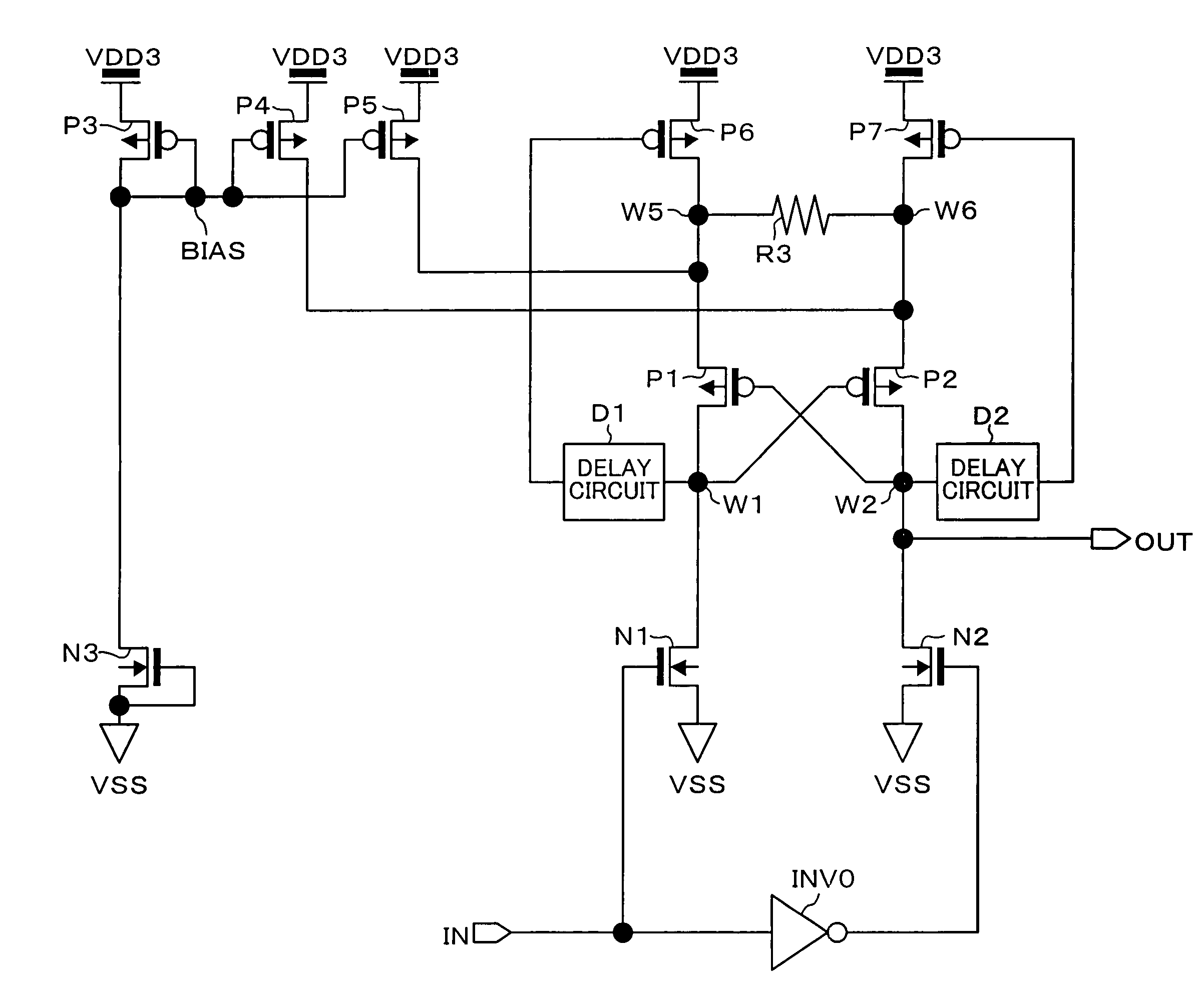
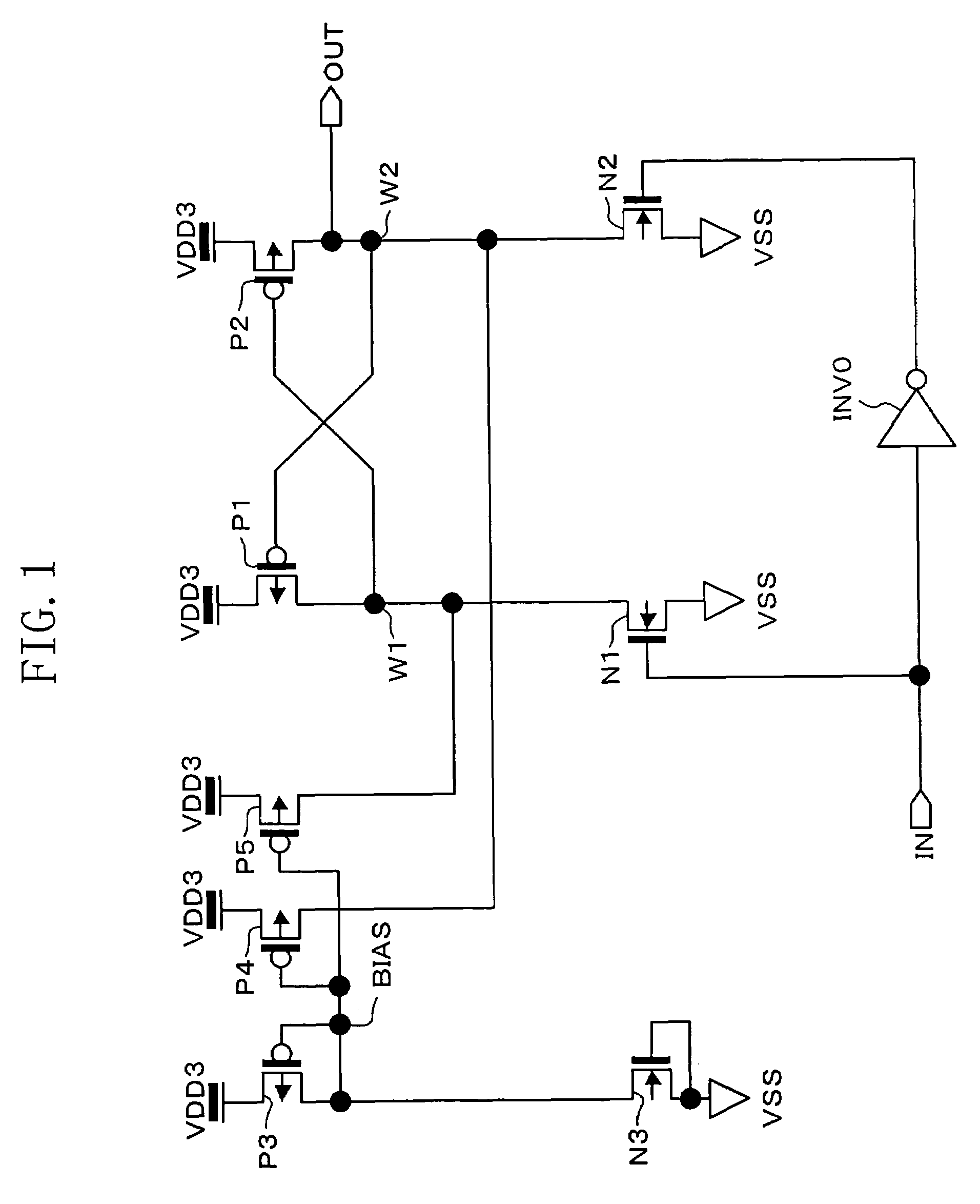
[0084]FIG. 1 shows a specific structure of a level shifter according to embodiment 1.
[0085]In FIG. 1, a terminal IN is a signal input terminal, an element INV0 is an inverter formed by a lower voltage side element for inverting a signal input through the input terminal IN. The inverter INV0 operates with lower voltage supply (first voltage supply) VDD of, for example, 1.5 V.
[0086]In FIG. 1, the elements other than the inverter INV0 are elements on the higher voltage side at, for example, 3.3 V. The level shifter includes a pair of N-type transistors N1 and N2 for complementary signal input, which has sources connected to the ground. The gate of the N-type transistor N1 (first first-conductivity type transistor) receives a signal input through the input terminal IN (one of complementary first and second input signals). The gate of the N-type transistor N2 (second first-conductivity type transistor) receives an output signal of the inverter INV0 (the other of the complementary first a...
embodiment 2
[0118]FIG. 5 shows a specific structure of a level shifter of embodiment 2.
[0119]The level shifter of FIG. 5 includes, in addition to the components of the level shifter of FIG. 1 of embodiment 1, a P-type transistor P8 which is provided in place of the P-type transistors P4 and P5. The source of the P-type transistor P8 is connected to higher voltage supply VDD3. The gate of the P-type transistor P8 is connected to the node BIAS. The P-type transistor P8 cooperates with the P-type transistor P3 as a current mirror and forms a current conversion circuit which amplifies the OFF leakage current flowing through the N-type transistor N3 by a predetermined factor to generate a current flowing from higher voltage supply VDD3. The level shifter of FIG. 5 further includes P-type transistors P9 and P10 which constitute a switch circuit for connecting the drain of the P-type transistor P8 to any one of the nodes W1 and W2. The sources of the P-type transistors P9 and P10 are connected to the ...
embodiment 3
[0125]FIG. 6 shows a specific structure of a level shifter of embodiment 3.
[0126]The level shifter of FIG. 6 is different from the level shifter of FIG. 5 of embodiment 2 in that the P-type transistor P10 is merged into the P-type transistor P1 and the P-type transistor P9 is merged into the P-type transistor P2. The drain of the P-type transistor P8 is connected to the sources of the P-type transistors P1 and P2. The P-type transistors P9 and P10 of FIG. 5 are not shown because they are merged into the P-type transistors P2 and P1, respectively. The other part of the structure is the same as that of embodiment 2.
[0127]The operation of the level shifter of embodiment 3 is the same as that of the level shifter of FIG. 5 of embodiment 2. The level shifter of embodiment 3 is formed by a smaller number of transistors than the level shifter of embodiment 2, and therefore, the same operation of the level shifter is realized with a smaller circuit area as compared with embodiment 2.
PUM
 Abstract
Description
Claims
Application Information


