Nonvolatile memories with charge trapping dielectric modified at the edges

a charge trapping dielectric and edge modification technology, applied in the field of charge trapping memories, can solve the problems of reducing data retention time, reducing reducing the insulation property of blocking dielectrics at the edges, so as to reduce the density of charge trapping sites, reduce the conductivity of charges, and reduce current leakage through blocking dielectric edges

Inactive Publication Date: 2010-03-11
PROMOS TECH PTE LTD
View PDF7 Cites 29 Cited by
  • Summary
  • Abstract
  • Description
  • Claims
  • Application Information

AI Technical Summary

Benefits of technology

[0006]The inventors have discovered, and experimentally confirmed, that the current leakage through the blocking dielectric edges can be reduced by modifying the composition of the charge-trapping dielectric at the edges adjacent to the edges of the blocking dielectric. For example, in some embodiments, the charge-trapping dielectric is formed of silicon-rich silicon nitride (“SiRN” hereinbelow). After the charge-trapping dielectric and the blocking dielectric have been patterned, the wafer is oxidized. Therefore, the edge portions of the charge-trapping dielectric are converted to silicon oxide and / or silicon oxynitride (SION). The oxidation reduces the density of the charge trapping sites at the edges of the charge trapping dielectric and hence reduces the conductivity of charges at the edges, thus reducing the charge and current leakage through the blocking dielectric edges (and through the tunnel dielectric edges).
[0007]Silicon-rich silicon nitride advantageously provides a higher density of charge-trapping sites than stoichiometric silicon nitride (Si3N4). The high density of trapping sites allows one to reduce the programming and erase times and / or the programming and erase voltages and to facilitate differentiation between memory states in the reading operation. However, the high density of trapping sites may increase the leakage current, making it particularly important that the leakage current be reduced. Further, in some dielectrics including aluminum oxide, the etch damage cannot be effectively annealed by heating, so reducing the edge leakage via modifying the charge-trapping dielectric is particularly appropriate.

Problems solved by technology

The insulating property of the blocking dielectric can be weakened at the edges by defects created when the blocking dielectric is patterned.
The resulting current leakage at the edges of the blocking dielectric makes it more difficult to control the state of the cell by the program and erase processes described above, and the charge leakage reduces the data retention time.
Further, in some dielectrics including aluminum oxide, the etch damage cannot be effectively annealed by heating, so reducing the edge leakage via modifying the charge-trapping dielectric is particularly appropriate.

Method used


Image

  • Nonvolatile memories with charge trapping dielectric modified at the edges
  • Nonvolatile memories with charge trapping dielectric modified at the edges
  • Nonvolatile memories with charge trapping dielectric modified at the edges

Examples


Embodiment Construction

[0020]The embodiments described in this section illustrate but do not limit the invention except as defined by the appended claims. In particular, the materials and dimensions given in this section are for illustration purposes only except as defined by the appended claims.

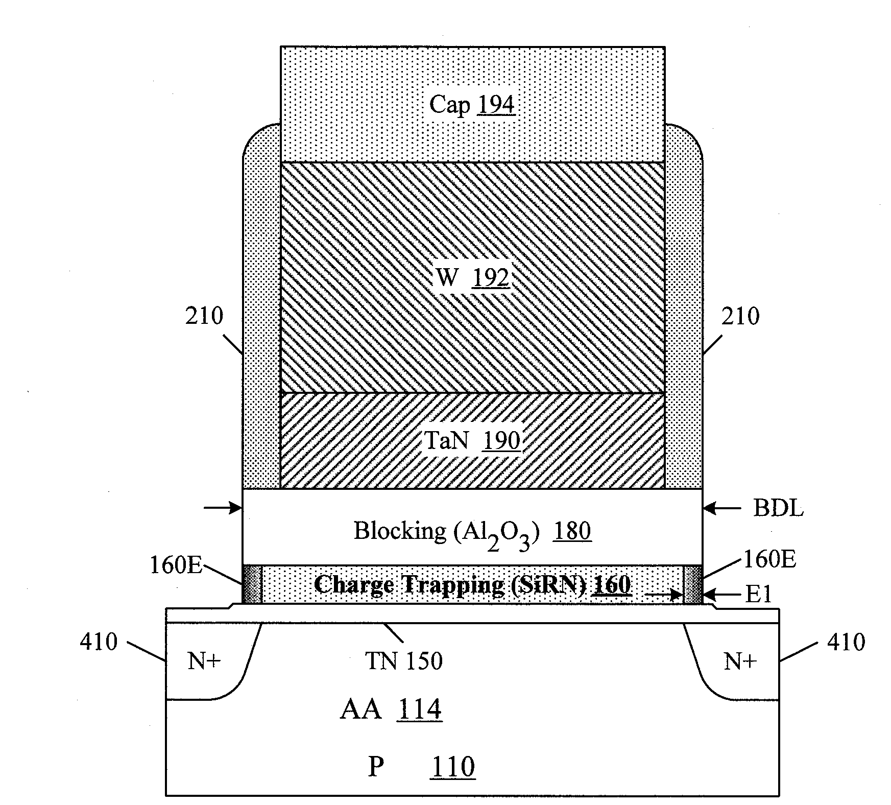
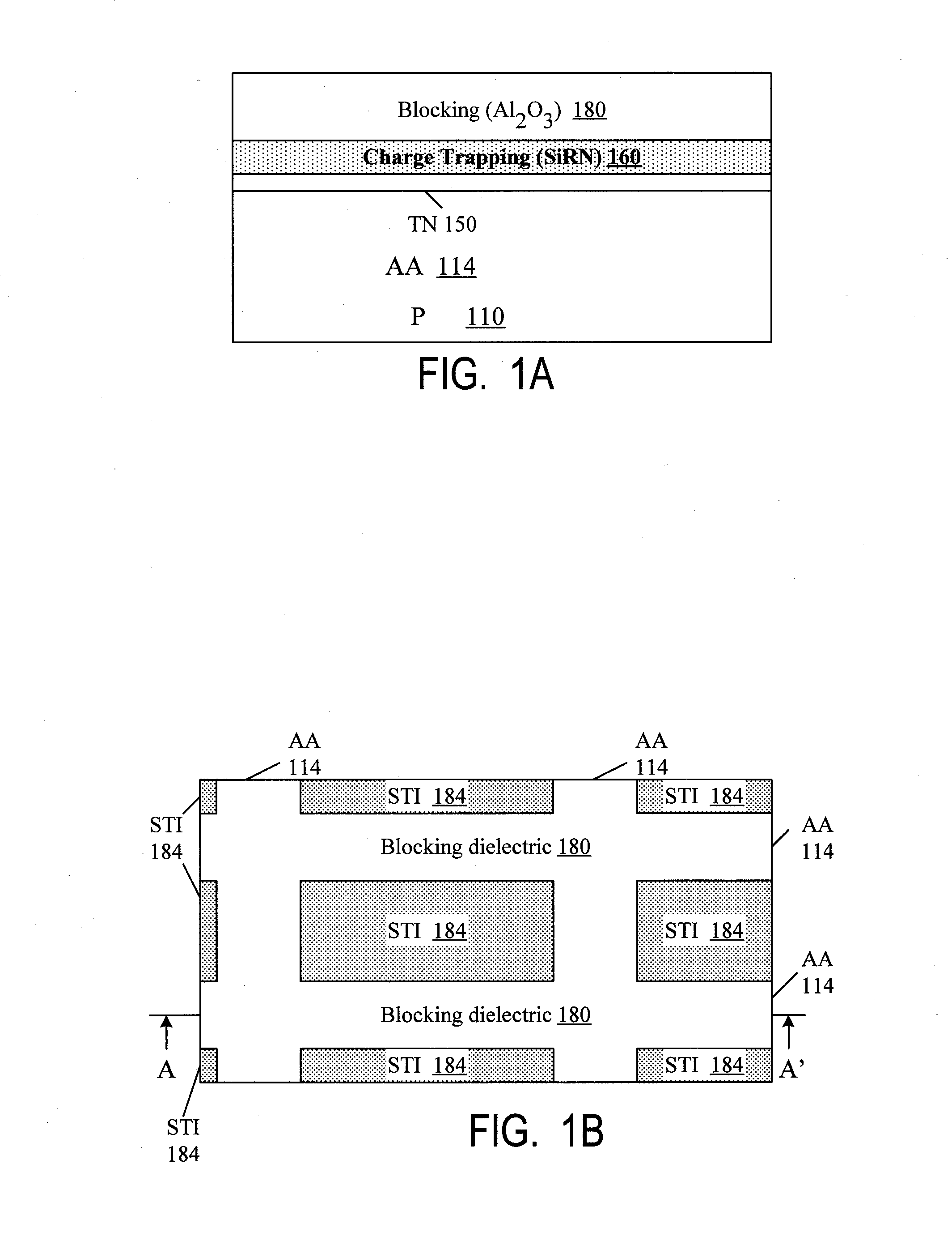
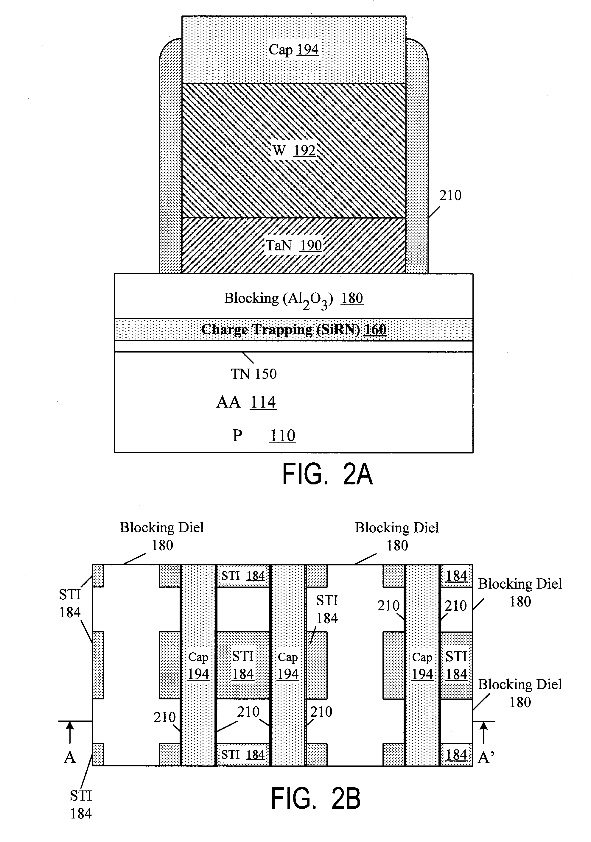
[0021]FIGS. 1A, 1B illustrates the beginning stages of fabrication of an array of memory cells which incorporate an embodiment of the present invention. The invention is not limited to an array or a particular array or cell architecture, and may include a single memory cell or any combination of such cells. FIG. 1A shows a vertical cross section along the line A-A′ shown in the top view FIG. 1B. FIGS. 1A, 1B are not drawn to the same scale. As shown in FIG. 1A, an isolated P well is formed in monocrystalline silicon substrate 110. The P well will include the memory cell's active area 114. Tunnel dielectric 150 is formed on the active area 114. In some exemplary, non-limiting embodiments, dielectric 150 is silicon ...


PUM


Abstract

A nonvolatile memory cell has charge trapping dielectric (160) which has been modified (i.e. oxidized) adjacent to edges of blocking dielectric (180). The modification reduces the charge-trapping density adjacent to the edges of the blocking dielectric, and hence reduces the leakage current at the edges. Other features are also provided.

Description

BACKGROUND OF THE INVENTION[0001]The present invention relates to charge-trapping memories.[0002]The state of a charge-trapping memory cell is defined by the electric charge stored in the cell's charge-trapping dielectric (e.g. silicon nitride). The charge-trapping dielectric is positioned between the cell's active area (a semiconductor area including the cell's channel and source / drain regions) and the control gate. The charge-trapping dielectric is insulated from the active area by tunnel dielectric (e.g. silicon dioxide). The memory state can be changed by electron transfer between the charge-trapping dielectric and the active area through the tunnel dielectric. For example, to program the memory cell, a positive voltage is applied to the control gate relative to the channel region to transfer electrons from the active area to the charge-trapping dielectric. To erase the memory cell, a negative voltage is applied to transfer electrons back to the active area.[0003]When electrons ...

Claims


Application Information

Patent Timeline
Patent Type & Authority Applications(United States)
IPC IPC(8): H01L29/00H01L21/3205
CPCH01L21/28282H01L27/11565H01L29/792H01L29/513H01L29/518H01L29/4234H01L29/40117H10B43/10
Inventor ZHENG, WEIFON, CHUNG WAH
Owner PROMOS TECH PTE LTD
Why Eureka
Try Eureka