Preparation method of Ge-based Metal Oxide Semiconductor (MOS) device with sub-nanometer equivalent to oxide thickness

A technology of oxide thickness and MOS devices, which is applied in semiconductor/solid-state device manufacturing, electrical components, circuits, etc., can solve problems such as hindering the preparation of Ge-based transistors, Fermi pinning effect, poor interface quality, etc., to reduce defect charges and interface state density, improved electrical properties, and reduced thickness

Inactive Publication Date: 2012-07-04
NANJING UNIV
View PDF1 Cites 7 Cited by
  • Summary
  • Abstract
  • Description
  • Claims
  • Application Information

AI Technical Summary

Problems solved by technology

However, the main factor restricting the large-scale application of germanium in integrated circuits is the lack of stable germanium oxide with a high-quality interface with germanium. The usual surface germanium oxide (GeO 2 and GeO) are either water-soluble or volatile, have very poor interface quality, and produce severe Fermi pinning effects, which greatly hinder the fabrication of Ge-based transistors, introducing high-k materials into Ge, for The development of Ge transistors provides a new opportunity

Method used


Image

  • Preparation method of Ge-based Metal Oxide Semiconductor (MOS) device with sub-nanometer equivalent to oxide thickness
  • Preparation method of Ge-based Metal Oxide Semiconductor (MOS) device with sub-nanometer equivalent to oxide thickness
  • Preparation method of Ge-based Metal Oxide Semiconductor (MOS) device with sub-nanometer equivalent to oxide thickness

Examples


Embodiment 1

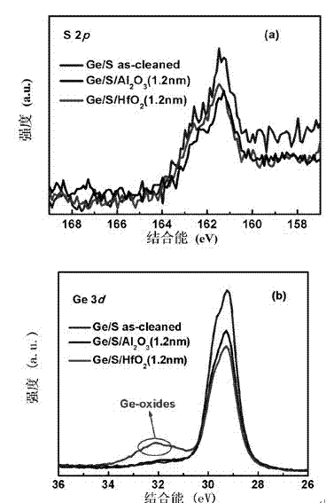
[0026] 1. Ge substrate cleaning and S passivation: The substrate material is a commercial single crystal germanium wafer, N type, orientation (100), resistivity 0.2-0.3 W cm. Sonicate with acetone and methanol for 5 minutes in turn to remove the oil on the Ge surface. HBr (HBr / H 2 O=1:3 weight ratio) Soak in aqueous solution for 5 minutes to remove the natural oxide layer on the surface. Then use 20% weight ratio (NH 4 ) 2 The S aqueous solution is soaked for 20 minutes to form a Ge-S bond on the Ge surface and further remove excess Ge oxides. Finally, rinse the treated germanium surface with deionized water, dry it with high-purity nitrogen, and put it into the ALD reaction chamber.

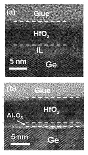
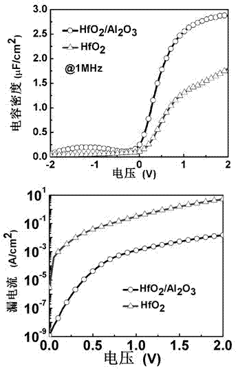
[0027] 2. Preparation of HfO by atomic layer deposition 2 / Al 2 o 3 Stacking structure film:

[0028] Growth temperature: 220 ℃; reaction source: trimethylaluminum (Al(CH 3 ) 3 TMA), four two (methyl ammonia) hafnium (Hf [N (CH 3 ) 2 ] 4, TDMAH), the oxygen source is water H 2 O;...

Embodiment 2

[0039] 1. Ge substrate cleaning and S passivation: The substrate material is a commercial single crystal germanium wafer, N type, orientation (100), resistivity 0.2-0.3 W cm. Use acetone and methanol to sonicate for 3 minutes in sequence to remove the oil on the Ge surface. HBr (HBr / H 2 O=1:3 weight ratio) Soak in aqueous solution for 3 minutes to remove the natural oxide layer on the surface. Then use 20% weight ratio (NH 4 ) 2 The S aqueous solution is soaked for 10 minutes to form a Ge-S bond on the Ge surface and further remove excess Ge oxides. Finally, rinse the treated germanium surface with deionized water, dry it with high-purity nitrogen, and put it into the ALD reaction chamber.

[0040] 2. Preparation of HfO by atomic layer deposition 2 / Al 2 o 3 Stacking structure film:

[0041] Growth temperature: 250 ℃; reaction source: trimethylaluminum (Al(CH 3 ) 3 TMA), tetrakis(methylethylammonia) hafnium (Hf[N(CH 3 )(C 2 h 5 )] 4, TEMAH), the oxygen source i...

Embodiment 3

[0046] 1. Ge substrate cleaning and S passivation: The substrate material is a commercial single crystal germanium wafer, N type, orientation (100), resistivity 0.2-0.3 W cm. Use acetone and methanol to sonicate for 10 minutes in sequence to remove the oil on the Ge surface. HBr (HBr / H 2 O=1:3 weight ratio) Soak in aqueous solution for 7 minutes to remove the natural oxide layer on the surface. Then use 20% weight ratio (NH 4 ) 2 Soak in aqueous solution of S for 40 minutes to form Ge-S bonds on the surface of Ge and further remove excess Ge oxides. Finally, rinse the treated germanium surface with deionized water, dry it with high-purity nitrogen, and put it into the ALD reaction chamber.

[0047] 2. Preparation of HfO by atomic layer deposition 2 / Al 2 o 3 Stacking structure film:

[0048] Growth temperature: 300 ℃; reaction source: trimethylaluminum (Al(CH 3 ) 3 TMA), tetrakis(methylethylammonia) hafnium (Hf[N(CH 3 )(C 2 h 5 )] 4, TEMAH), the oxygen source i...


PUM

PropertyMeasurementUnit
thicknessaaaaaaaaaa

Abstract

The invention discloses a preparation method of a Ge-based Metal Oxide Semiconductor (MOS) device with sub-nanometer equivalent to oxide thickness, comprising the steps of 1) cleaning a Ge substrate; 2), performing S passivating; 3), depositing an Al2O3 film on the surface of the Ge substrate in situ;4), depositing an HfO2 film; 5), putting the substrate to a quick annealing furnace to anneal to obtain a finished product. The method obtains a thin aluminum oxide film by in-situ atomic layer deposition, improves interface quality of a gate dielectric film and the Ge substrate, notably improves the electric property of the gate dielectric film and obtains Ge-based MOS device with the Equivalent Oxide Thickness (EOT) of less than 1nm and the leakage current density of less than 2mA/cm2.

Description

[0001] technical field [0002] The invention relates to a method for preparing a MOS device, in particular to a method for preparing a MOS device with an equivalent oxide thickness of sub-nanometer on an S-passivated Ge substrate by using atomic layer deposition technology. Background technique [0003] As the size of devices continues to shrink, the development of gate dielectric film preparation technology compatible with existing metal-oxide-semiconductor field-effect transistors (MOSFETs) technology is an important issue in the field of microelectronics. Task. Atomic Layer Deposition (ALD) is a chemical vapor deposition technology that can precisely control the thickness of the sub-monolayer (sub-monolayer), and is receiving more and more attention. It is used in deep submicron integrated circuits. And the preparation of nanostructures shows great application prospects. [0004] high k The introduction of gate dielectric and metal gate materials, while reducing the...

Claims


Application Information

Patent Timeline
Patent Type & Authority Applications(China)
IPC IPC(8): H01L21/336H01L21/283
Inventor 李爱东李学飞曹燕强吴迪
Owner NANJING UNIV
Why Eureka
Try Eureka