Semiconductor device with heterojunction

a technology of semiconductor devices and heterojunctions, applied in the field of semiconductor devices, can solve the problems of increasing the leakage current from the heterojunction interface, the difficulty of achieving a high withstand voltage and a low on-resistance, etc., to achieve the effect of improving the driving force of transistors, lowering the barrier height, and increasing the leakage curren

Active Publication Date: 2005-09-15
NISSAN MOTOR CO LTD
View PDF3 Cites 28 Cited by
  • Summary
  • Abstract
  • Description
  • Claims
  • Application Information

AI Technical Summary

Benefits of technology

[0004] The field-effect transistor of the disclosure mentioned above, however, has a trade-off problem that lowering the barrier height of the heterojunction to improve transistor driving force results in increasing a leakage current from the heterojunction interface when applying a high voltage between the source electrode and the drain electrode. Namely, the related art has a difficulty in simultaneously realizing a high withstand voltage and a low ON-resistance through the optimization of the barrier height of a heterojunction. In view of the problem, the present invention is to provide a semiconductor device capable of achieving a low ON-resistance, small leakage current, and high withstand voltage.

Problems solved by technology

The field-effect transistor of the disclosure mentioned above, however, has a trade-off problem that lowering the barrier height of the heterojunction to improve transistor driving force results in increasing a leakage current from the heterojunction interface when applying a high voltage between the source electrode and the drain electrode.
Namely, the related art has a difficulty in simultaneously realizing a high withstand voltage and a low ON-resistance through the optimization of the barrier height of a heterojunction.

Method used


Image

  • Semiconductor device with heterojunction
  • Semiconductor device with heterojunction
  • Semiconductor device with heterojunction

Examples


first embodiment

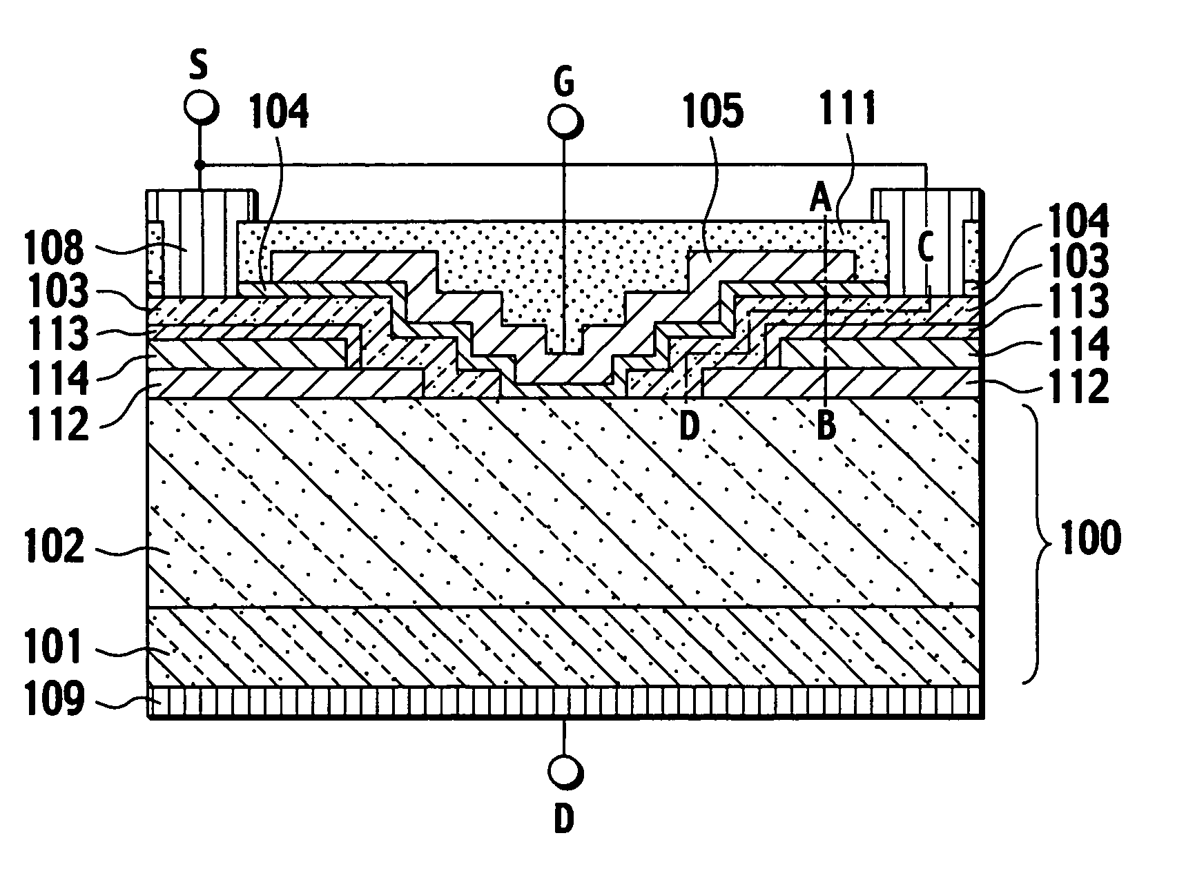
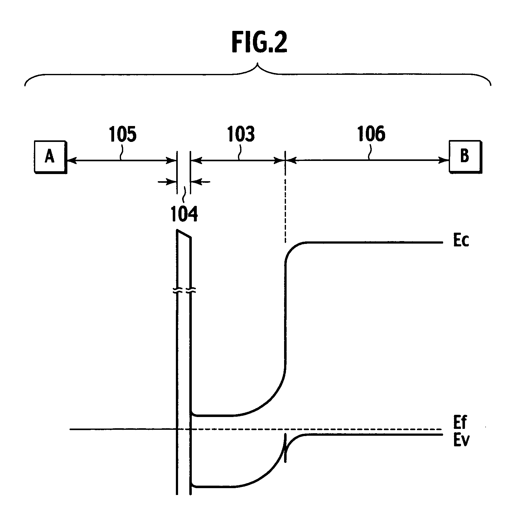
[0017]FIG. 1 is a sectional view showing a semiconductor device according to a first embodiment of the present invention. The semiconductor device has an n-type silicon carbide substrate 101 and an n-type silicon carbide epitaxial layer 102 whose impurity concentration is lower than that of the substrate 101. The substrate 101 and epitaxial layer 102 form a silicon carbide semiconductor base 100 made of n-type silicon carbide. Here, silicon carbide serves as a first semiconductor material and n-type serves as a first conductivity type. The semiconductor base 100 forms a heterojunction with a hetero-semiconductor region 103 made of n-type polycrystalline silicon. Here, polycrystalline silicon serves as a second semiconductor material and has a band gap different from that of silicon carbide. A first gate electrode 105 is formed on a first gate insulating film 104 in the vicinity of the heterojunction formed between the epitaxial layer 102 and the hetero-semiconductor region 103. A p-...

second embodiment

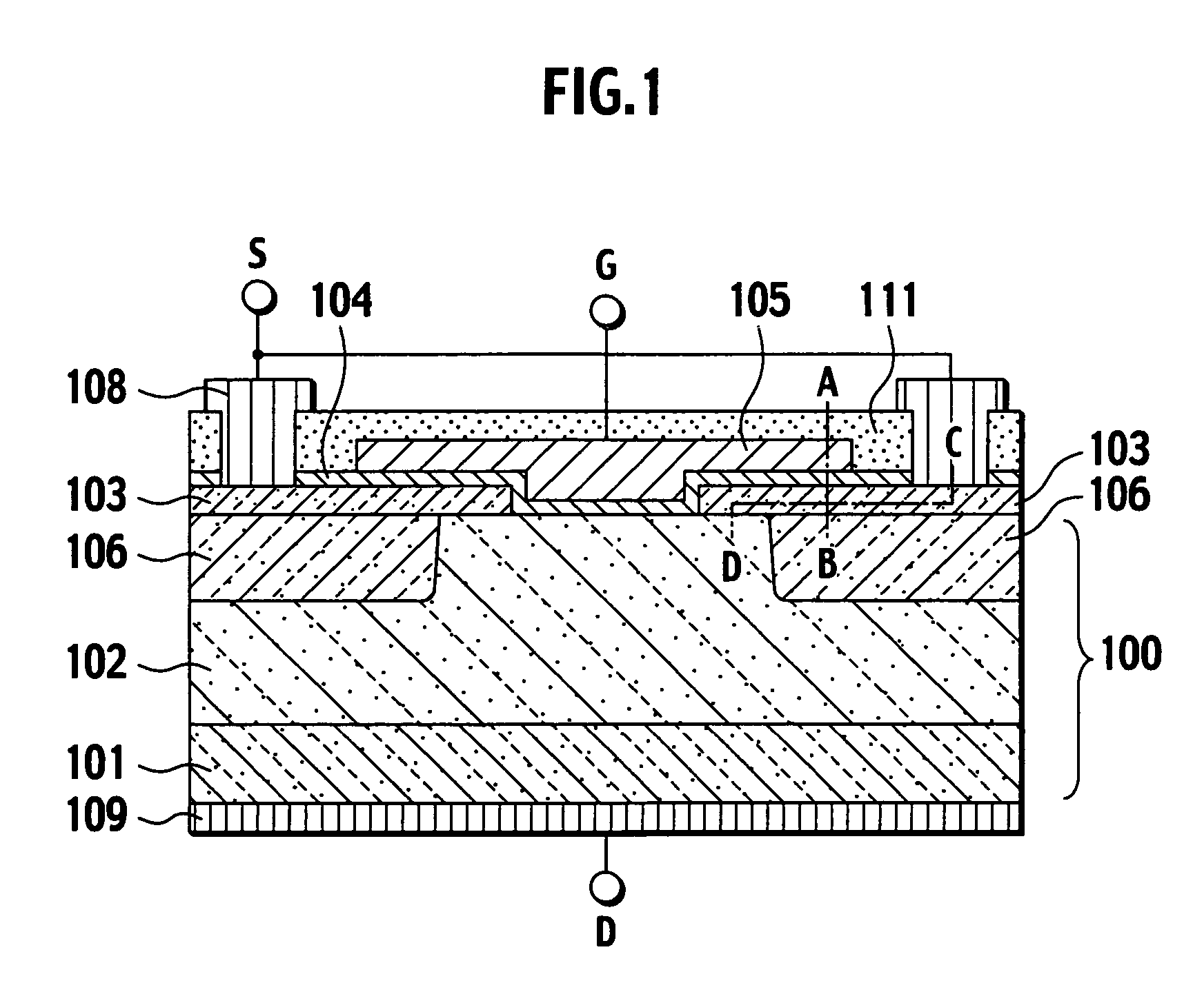
[0030] In the first embodiment, the part that extends a built-in electric field into the hetero-semiconductor region 103 is a part of the p-type silicon carbide region 106. Instead of the p-type silicon carbide region 106, the second embodiment employs metal whose work function is greater than that of the first semiconductor material (silicon carbide) having the first conductivity type (n-type) and that of the second semiconductor material (polycrystalline silicon).

[0031]FIG. 5 is a sectional view showing a semiconductor device according to the second embodiment. The semiconductor device includes an n-type silicon carbide substrate 101 and an n-type silicon carbide epitaxial layer 102 whose impurity concentration is lower than that of the substrate 101. The substrate 101 and epitaxial layer 102 form a silicon carbide semiconductor base 100 made of n-type silicon carbide. Here, silicon carbide is a first semiconductor material and n-type is a first conductivity type. The semiconduct...

third embodiment

[0036]FIG. 7 is a sectional view showing a semiconductor device according to a third embodiment of the present invention. In FIG. 7, a silicon carbide semiconductor base 100 includes an n-type silicon carbide substrate 101 and an n-type silicon carbide epitaxial layer 102 whose impurity concentration is lower than that of the substrate 101. The semiconductor base 100 forms a heterojunction with a hetero-semiconductor region 103 made of polycrystalline silicon serving as a second semiconductor material whose band gap is different from that of silicon carbide. Adjacent to the heterojunction formed by the epitaxial layer 102 and hetero-semiconductor region 103, there is a first gate insulating film 104 on which a first gate electrode 105 is formed. Facing the first gate electrode 105 through the hetero-semiconductor region 103 and first gate insulating film 104, there is an insulated gate region consisting of a second gate insulating film 113 and a second gate electrode 114. A source e...


PUM


Abstract

An aspect of the present invention provides a semiconductor device that includes a semiconductor base made of a first semiconductor material of a first conductivity type, a hetero-semiconductor region forming a heterojunction with the semiconductor base and made of a second semiconductor material having a different band gap from the first semiconductor material, a first gate electrode arranged in the vicinity of the heterojunction, a first gate insulating film configured to insulate the first gate electrode from the semiconductor base, a source electrode formed in contact with the hetero-semiconductor region, a dram electrode formed in contact with the semiconductor base, and an electric field extending region partly facing the first gate electrode, the first gate insulating film and hetero-semiconductor region interposed between the electric field extending region and the first gate electrode, the electric field extending region extending a built-in electric field into the hetero-semiconductor region.

Description

BACKGROUND OF THE INVENTION [0001] The present invention relates to a semiconductor device, and particularly, to a semiconductor device having a heterojunction. [0002] Silicon carbide has one digit larger dielectric breakdown strength than silicon and is processible by thermal oxidization like silicon. Due to this, silicon carbide is drawing attention as a next generation semiconductor material. In particular, silicon carbide is expected for application to power conversion devices. Recently those devices made of silicon carbide are high-withstand-voltage, low-loss power transistors. To reduce a loss from a power transistor, the ON-resistance of the power transistor must be lowered. [0003] As an example of an ON-resistance reduced power transistor, Japanese Laid-Open Patent Publication No. 2003-218398 discloses a field-effect transistor. The disclosed field-effect transistor includes a hetero-semiconductor region and a silicon carbide epitaxial layer that form a heterojunction. The d...

Claims


Application Information

Patent Timeline
Patent Type & Authority Applications(United States)
IPC IPC(8): H01L21/336H01L29/06H01L29/12H01L29/24H01L29/267H01L29/47H01L29/78H01L29/732H01L31/0328H01L31/0336H01L31/072H01L31/109
CPCH01L29/7813H01L29/0619H01L29/7828H01L29/47H01L29/7827H01L29/267
Inventor TANAKA, HIDEAKIHOSHI, MASAKATSUHAYASHI, TETSUYA
Owner NISSAN MOTOR CO LTD
Why Eureka
Try Eureka