Fin FET (field effect transistor) and manufacturing method of fin FET

A fin-type field effect and manufacturing method technology, which is applied in semiconductor/solid-state device manufacturing, semiconductor devices, electrical components, etc., can solve the problems of reduced driving current and increased leakage current, so as to reduce height, improve driving ability, reduce The effect of source-drain resistance

Active Publication Date: 2013-09-18
锐立平芯微电子(广州)有限责任公司
View PDF5 Cites 5 Cited by
  • Summary
  • Abstract
  • Description
  • Claims
  • Application Information

AI Technical Summary

Problems solved by technology

[0005] However, due to the high source/channel Schottky barrier height (SBH) of traditional Schottky barrier (SB) MOSFETs in the

Method used


Image

  • Fin FET (field effect transistor) and manufacturing method of fin FET
  • Fin FET (field effect transistor) and manufacturing method of fin FET
  • Fin FET (field effect transistor) and manufacturing method of fin FET

Examples


Example Embodiment

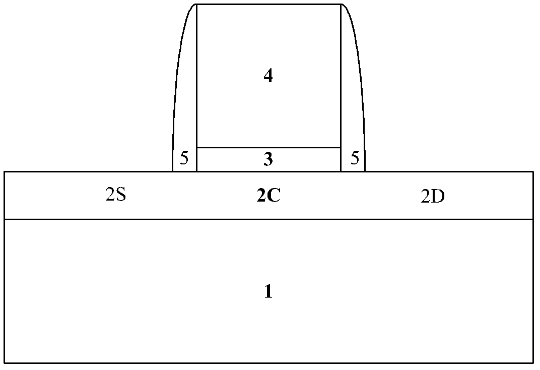
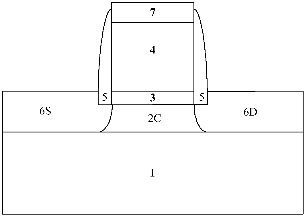
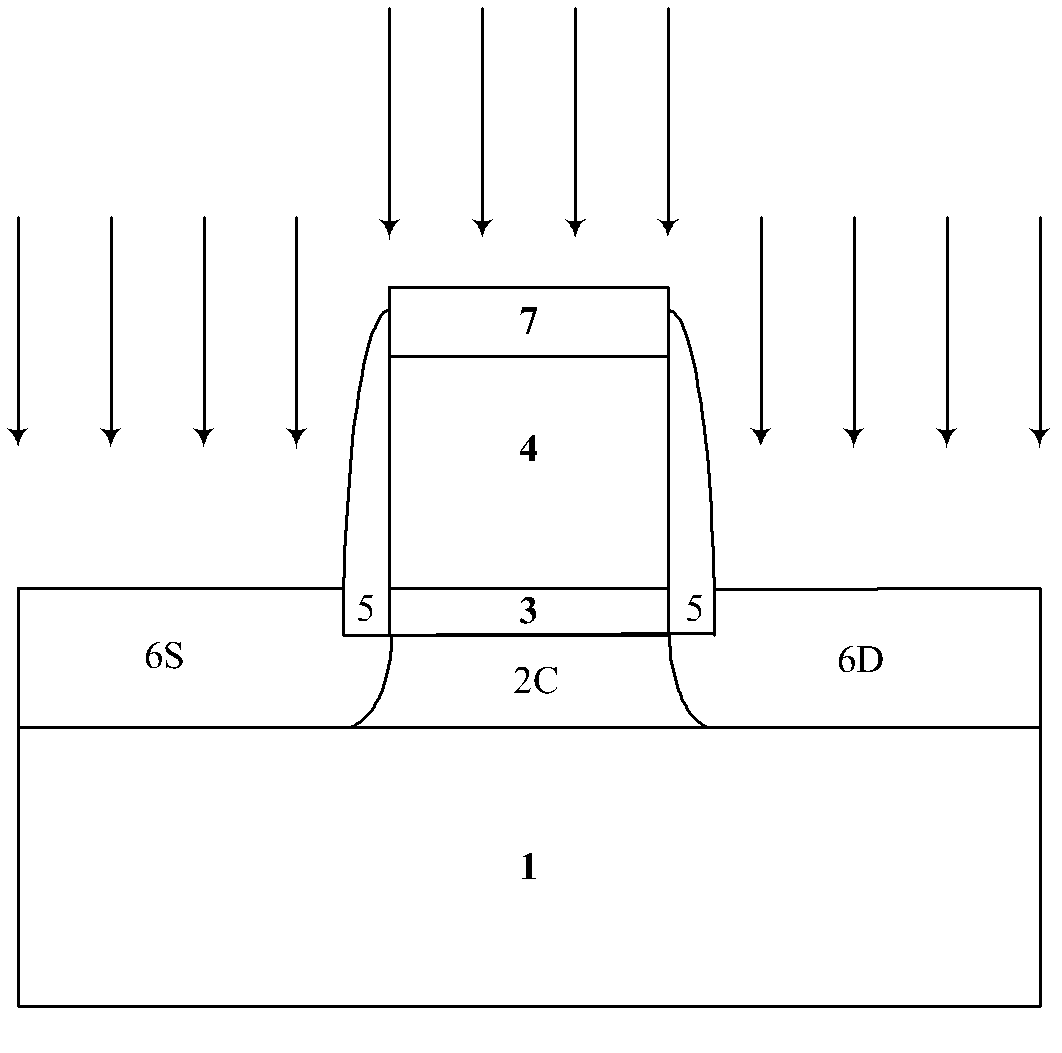
[0034] The features and technical effects of the technical solution of the present invention will be described in detail below with reference to the drawings and in conjunction with illustrative embodiments, and a novel FinFET device that can effectively reduce the source-drain resistance and improve the driving capability is disclosed. It should be pointed out that similar reference signs indicate similar structures. The terms "first", "second", "upper", "lower", etc. used in this application can be used to modify various device structures or manufacturing processes. . Unless otherwise specified, these modifications do not imply the spatial, order, or hierarchical relationship of the modified device structure or manufacturing process.

[0035] The present invention provides a method for manufacturing a novel FinFET device that can effectively reduce the source and drain resistance while improving the driving capability. The flowchart is Figure 5 Shown. Specifically refer to F...


PUM

PropertyMeasurementUnit
Thicknessaaaaaaaaaa

Abstract

The invention discloses a fin FET (field effect transistor), which comprises an SOI (silicon on insulator) substrate, a fin-shaped grid electrode stack structure and a channel region, wherein the fin-shaped grid electrode stacking structure is arranged on the SOI substrate, the channel region is arranged between a source drain region and a source drain region arranged at the two sides of the grid electrode stacking structure in the SOI substrate, the source drain regions and the channel region extend in the first direction, and the grid electrode stacking structure extends in the second direction vertical to the first direction. The fin FET is characterized in that the source drain regions are metal silicide, the interface part between the source drain regions and the channel region also comprises doping ion segregation regions. According to the novel fin FET device and a manufacturing method of the novel fin FET device provided by the invention, doping ions are filled into the source drain of the metal silicide of the Fin FET, in addition, the annealing driving is carried out so that the doping ions are segregated at the interface part of the channel region, the fin FET source and drain resistance is effectively reduced, and meanwhile, the Schottky barrier height is also reduced, so the driving capability is improved.

Description

technical field [0001] The invention relates to a semiconductor device and a manufacturing method thereof, in particular to a fin field effect transistor capable of effectively reducing the Schottky barrier height and a manufacturing method thereof. Background technique [0002] The quasi-planar multi-gate FinFET (Fin Field Effect Transistor) structure compatible with the traditional production process has a thin gate Spacer and a strong gate-controlled source-drain electric field, which suppresses the short-channel effect, reduces the channel doping concentration, and achieves low off-state current and high drive current characteristics. For SOI substrates, lower loff can be obtained due to the reduction of source-drain and substrate leakage paths, and the fully depleted ultra-thin body structure reduces junction capacitance and good sub-threshold characteristics, and sub-10nm gate length devices can be realized. [0003] However, in the existing quasi-planar multi-gate Fi...

Claims


Application Information

Patent Timeline
IPC IPC(8): H01L29/78H01L29/10H01L21/336H01L21/265
Inventor 尚海平徐秋霞
Owner 锐立平芯微电子(广州)有限责任公司
Why Eureka
Try Eureka