
Structure and manufacturing method of photomask read-only memory with low n-type buried source-drain resistance

A technology of read-only memory and source-drain resistance, applied in semiconductor/solid-state device manufacturing, electric solid-state devices, circuits, etc., can solve the problem of narrow current path, large RC delay in reading signal speed, and limited read-only memory of mask type Take current and other issues to achieve the effect of reducing source-drain resistance and increasing depth

Active Publication Date: 2018-08-21
SHANGHAI HUAHONG GRACE SEMICON MFG CORP
View PDF5 Cites 0 Cited by
  • Summary
  • Abstract
  • Description
  • Claims
  • Application Information

AI Technical Summary

Problems solved by technology

At the same time, the gate, source and drain are long strips, and the current path is narrow and long, which greatly limits the read current of the mask type read-only memory, and the circuit is also limited in the speed of reading signals (the RC delay is large )

Method used


Image

  • Structure and manufacturing method of photomask read-only memory with low n-type buried source-drain resistance
  • Structure and manufacturing method of photomask read-only memory with low n-type buried source-drain resistance
  • Structure and manufacturing method of photomask read-only memory with low n-type buried source-drain resistance

Examples


Embodiment Construction

[0020] In order to have a more specific understanding of the technical content, characteristics and effects of the present invention, now in conjunction with the accompanying drawings, the details are as follows:

[0021] The manufacturing method of the photomask type read-only memory of the low N-type buried source-drain resistance of the present invention, its specific process steps are as follows:

[0022] Step 1, forming shallow isolation trenches on the active area of ​​the silicon substrate to isolate the mask-type read-only memory area from peripheral circuits, such as Figure 4 shown.

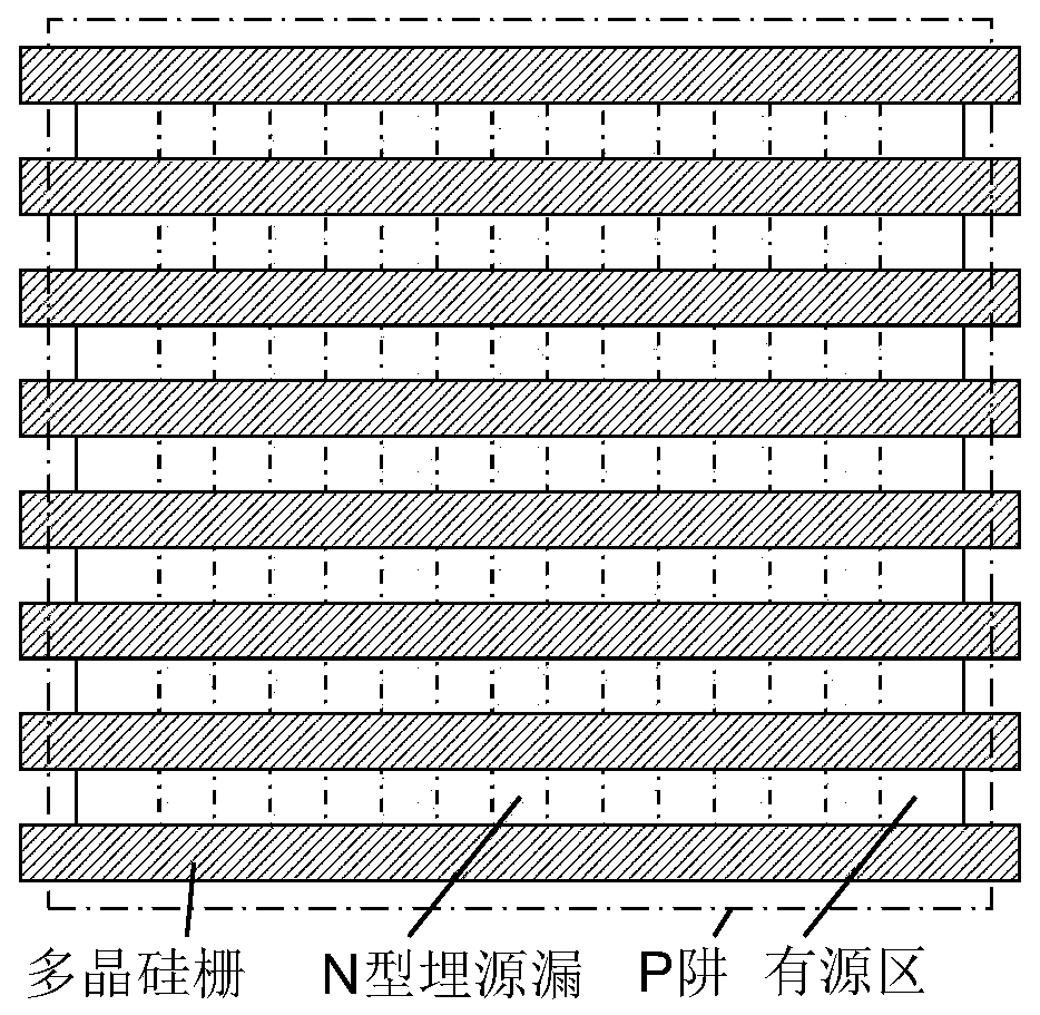
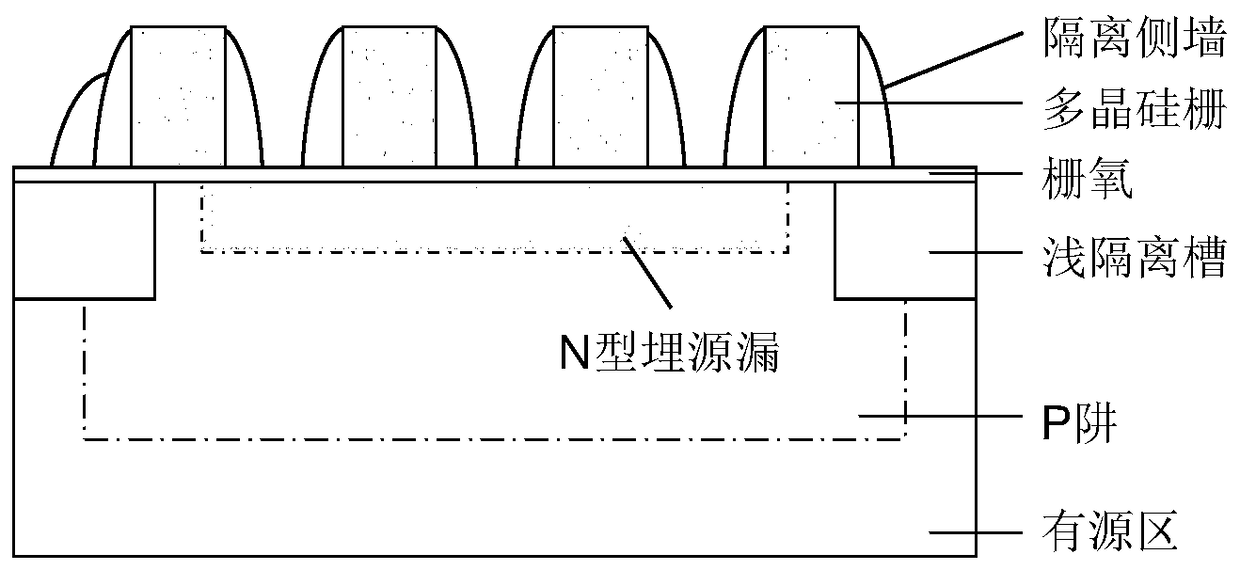
[0023] Step 2, perform P well implantation in the active area of ​​the mask type ROM to form the active area in the P well, such as Figure 5 (Figure B is the top view after this step is completed).

[0024] Step 3, coating the first photoresist outside the area where the first N-type buried source and drain is to be formed, the distance between the first photoresists, that is, the cr...


PUM


Abstract

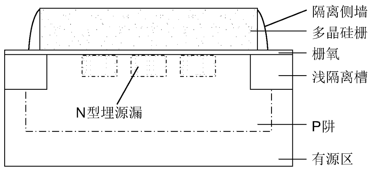
The invention discloses a manufacturing method of a mask read-only memory with low-N-type buried source-drain resistance. The method comprises the steps that (1), shallow isolation grooves are formed, and P-well injection is carried out; (2), light resistors of first N-type buried source-drains are coated, the distance between the light resistors is smaller than the target size, exposure is carried out, injection of arsenic ions or phosphonium ions is carried out, and the first N-type buried source-drains are formed; (3), a part of light resistors are removed, and the distance between the light resistors is made to be equal to the target size; (4), injection of arsenic ions is carried out, and second N-type buried source-drains connected with the first N-type buried source-drains are formed; (5), gate-oxide, polysilicon gates and grid electrode isolation side walls are formed. The invention further discloses the structure of the mask read-only memory manufactured through the method. The method of twice injection is adopted, the N-type buried source-drains of the special T-shaped structure are formed, the depth of the source-drains is increased under the conditions that the width of the source-drains is kept unchanged and the effective channel length is not affected, and therefore source-drain resistance of the mask read-only memory is lowered.

Description

technical field [0001] The invention relates to the field of integrated circuit manufacturing, in particular to the structure of a mask type read-only memory and its manufacturing method. Background technique [0002] Read-Only Memory (Read-Only Memory) is a memory that can only read data. The data of this memory is written at the time of production. In the manufacturing process, the data is burned into the circuit with a special mask (mask), so it is sometimes called "mask ROM" (mask ROM). In fact, it is very similar to the principle of a CD disc, in which the data state is written in the photolithography process of the semiconductor. [0003] The data of this mask-type read-only memory cannot be changed after writing, so the data cannot be lost, and its manufacturing cost is very low. Therefore, in devices that do not require data update, Mask ROM is very widely used use. [0004] However, the technical disadvantages of this mask-type ROM are also very obvious. Such a...

Claims


Application Information

Patent Timeline
Patent Type & Authority Patents(China)
IPC IPC(8): H01L27/112H01L21/8246
Inventor 刘冬华石晶段文婷钱文生
Owner SHANGHAI HUAHONG GRACE SEMICON MFG CORP
Learn More