Silicon/germanium-silicon vertical nodded type field effect transistor

A field-effect transistor, junction technology, used in transistors, semiconductor/solid-state device manufacturing, semiconductor devices, etc., can solve problems such as size limits

Inactive Publication Date: 2006-07-05
IBM CORP
View PDF8 Cites 0 Cited by
  • Summary
  • Abstract
  • Description
  • Claims
  • Application Information

AI Technical Summary

Problems solved by technology

However, when the gate length of the transistor is less than 0.1 microns or les

Method used


Image

  • Silicon/germanium-silicon vertical nodded type field effect transistor
  • Silicon/germanium-silicon vertical nodded type field effect transistor
  • Silicon/germanium-silicon vertical nodded type field effect transistor

Examples


Embodiment Construction

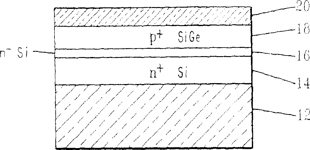
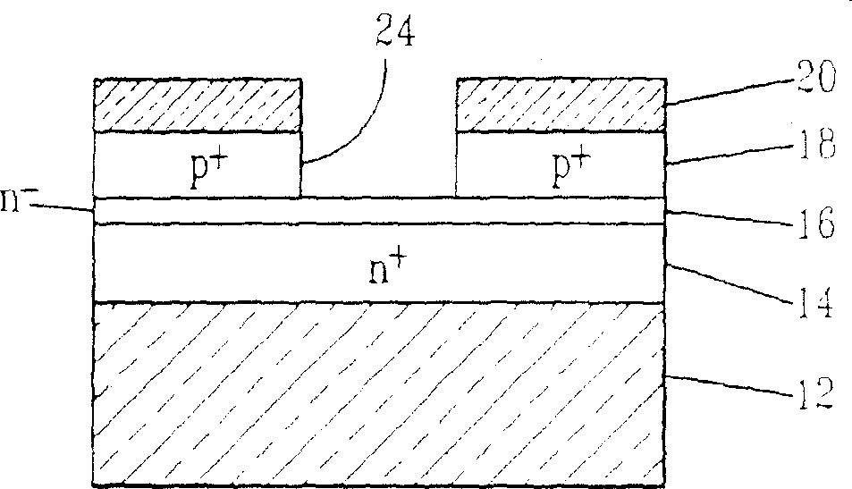
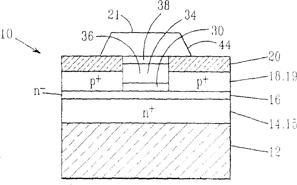
[0026] Referring now to the accompanying drawings, in particular Figure 1-3 , shows the steps of fabricating a vertical junction field effect transistor (JFET) 10 . The starting substrate 12 may be an insulator such as silicon dioxide, or the substrate 12 may be a semiconductor such as monocrystalline silicon, silicon germanium, or silicon-on-insulator. On the substrate 12 may be formed a p-doped semiconductor single crystal layer 14, such as silicon or silicon germanium. The starting substrate 12, if an insulator, and the layer 14 can be formed by isolation by implantation of oxygen (SIMOX), which is well known in the art, or by bonding and etching back an oxide-coated wafer and a semiconductor carrier substrate to Silicon-on-insulator (BESOI) is formed. Layer 14 may be a heavily doped n+ layer to form image 3 Drain electrode 15 of JFET 10 is shown.

[0027] Epitaxial layer 16 is formed on layer 14 , which may be a doped n-layer to reduce the capacitance of gate layer 18...


PUM

PropertyMeasurementUnit
Thicknessaaaaaaaaaa

Abstract

A junction field effect transistor and method for making is described incorporating horizontal semiconductor layers within an opening to form a channel and a semiconductor layer through which the opening was made which forms a gate electrode surrounding the channel. The horizontal semiconductor layers may be a SiGe alloy with graded composition near the source and drain. The invention overcomes the problem of forming low resistance JFET's and provides a gate length that is easily scaleable to submicron dimensions for rf, microwave, millimeter and logic circuits without short channel effects.

Description

field of invention [0001] This invention relates to junction field effect transistors, and more particularly to junction field effect transistors with a vertical channel of a graded SiGe alloy that provides strain for increased mobility and provides An induced electric field accelerates the charge carriers into the channel. technical background [0002] In standard metal-oxide-silicon (MOS) processes, enhancements in the speed of field effect transistors are usually accompanied by a reduction in device size. However, when the gate length of the transistor is less than 0.1 micron or less, there is a size limit because various other parameters cannot be scaled down. Short channel effects become important, but also inertial effects that cause carriers (electrons) to move at a low speed at the source of the channel become important. [0003] In US Patent 5,019,882, issued May 28, 1991 to P.M. Solomon, a field effect transistor containing a layer of silicon germanium used as a ...

Claims


Application Information

Patent Timeline
IPC IPC(8): H01L29/80H01L21/337H01L29/10H01L29/808
CPCH01L29/1058H01L29/66916H01L29/8086H01L29/8083Y10S438/936H01L29/772
Inventor K·E·伊斯迈尔B·S·梅耶尔森
Owner IBM CORP
Why Eureka
Try Eureka