

Micro optical sensor device
- Summary
- Abstract
- Description
- Claims
- Application Information
AI Technical Summary
Benefits of technology
Problems solved by technology
Method used
Image

Examples
Embodiment Construction
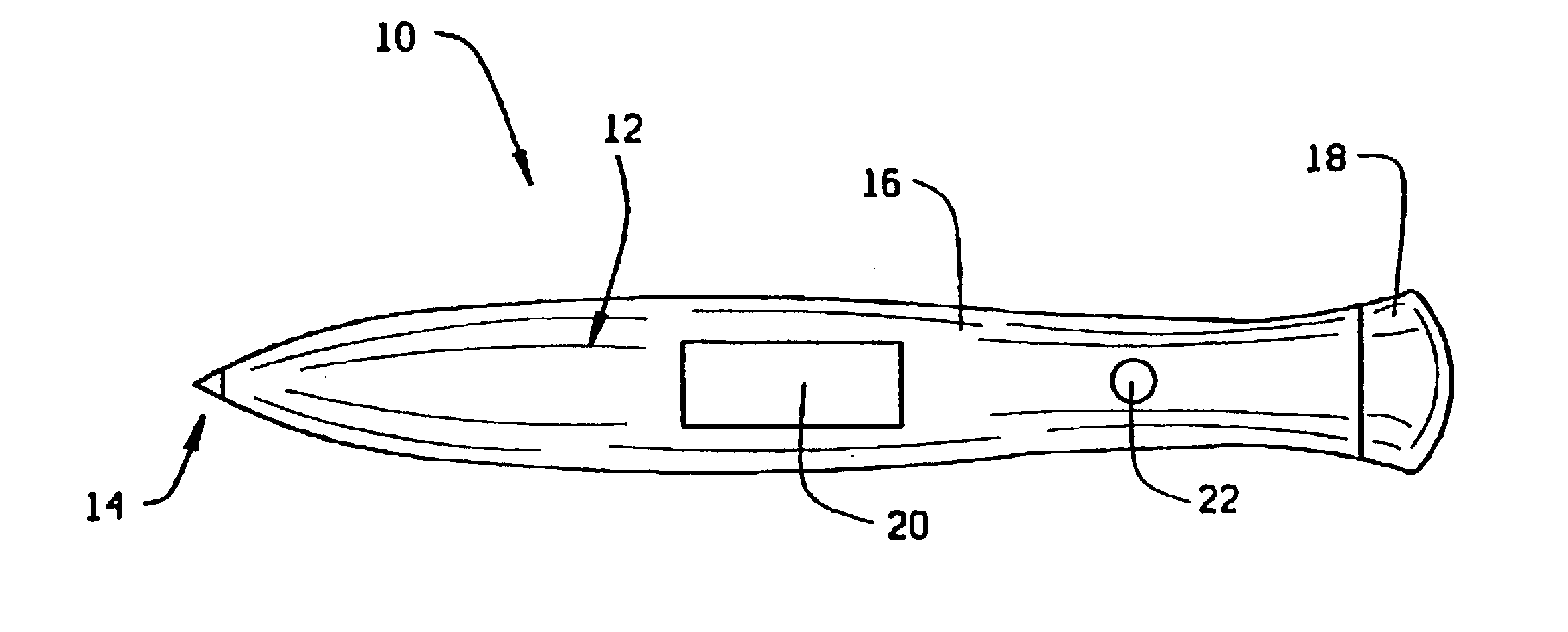
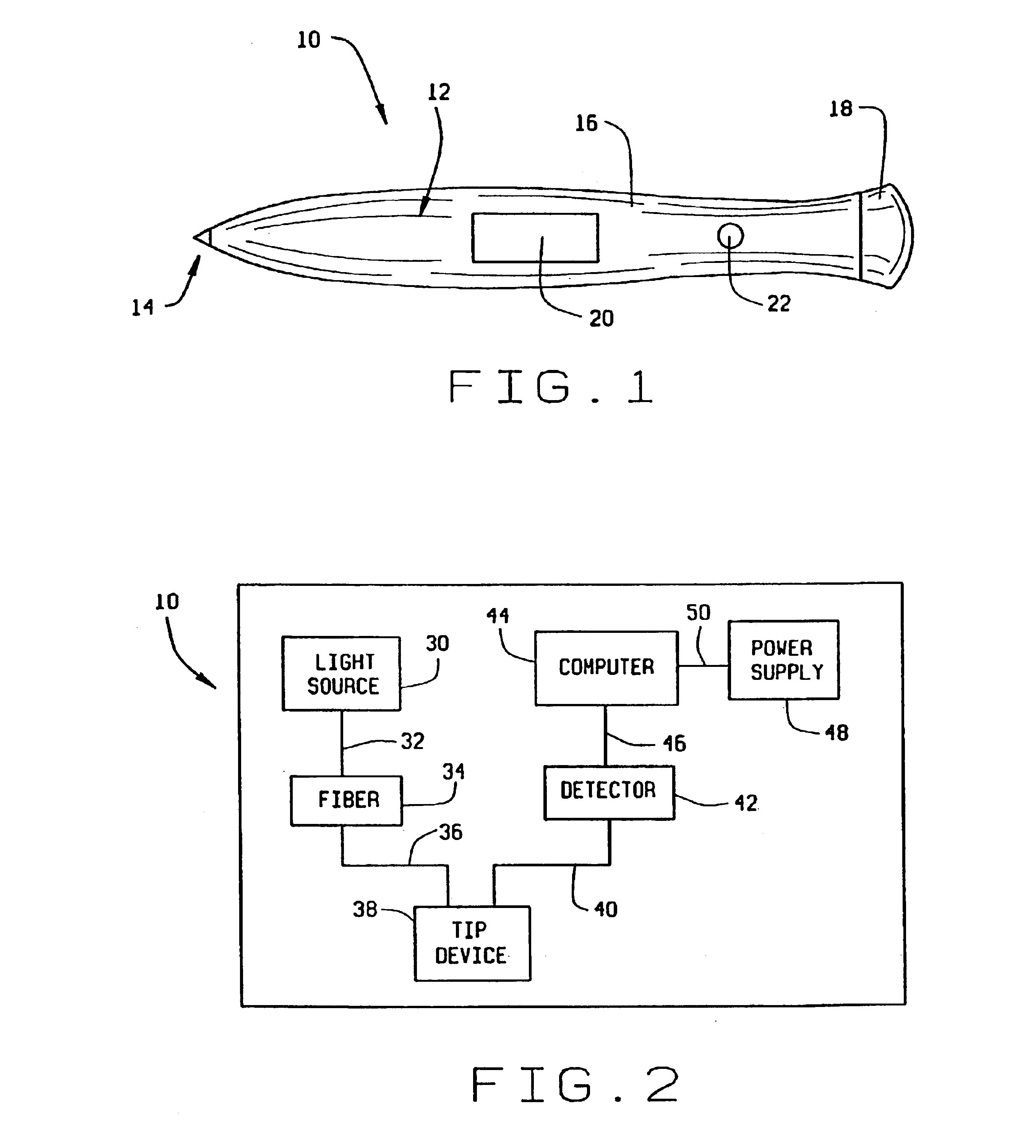
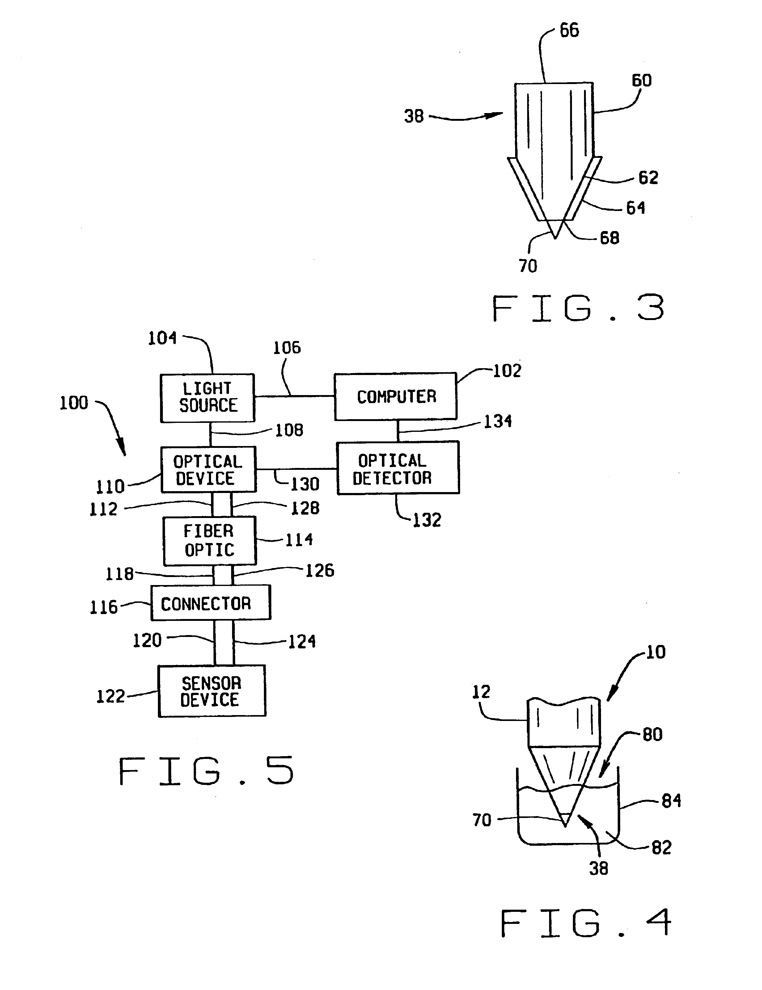
[0022]Referring now to the drawings, wherein like numbers refer to like items, number 10 identifies a preferred embodiment of a micro optical sensor device constructed according to the present invention. As illustrated in FIG. 1, the device 10 comprises a pencil or pen shaped body 12 which includes a tip portion 14, a central body portion 16, and an end cap 18. The central body portion 16 further includes a display device 20, such as an LED (light emitting diode) type display or an LCD type display, for displaying information. The end cap 18, which may be removable from the central body portion 16, is used to allow access into the interior of the central body portion 16. Batteries (not shown) can be inserted into the central body portion 16 to supply power to the device 10, as will be explained. The central body portion 16 may also include an ON / OFF switch 22 which may be used to operate the device 10. Other switches (not shown) may be incorporated into the central body portion 16 t...
PUM
| Property | Measurement | Unit |
|---|---|---|
| Diameter | aaaaa | aaaaa |
| Diameter | aaaaa | aaaaa |
| Diameter | aaaaa | aaaaa |
Abstract
Description
Claims
Application Information