Three-dimensional semiconductor device and manufacturing method thereof

一种器件制造方法、半导体的技术,应用在半导体/固态器件制造、半导体器件、电固体器件等方向,能够解决感应效率降低、数据无法读取、串联电阻上升等问题,达到提高感应效率和强度、提高读取电流和读取速度、减小源漏电阻的效果

Active Publication Date: 2017-07-11
INST OF MICROELECTRONICS CHINESE ACAD OF SCI
View PDF4 Cites 0 Cited by
  • Summary
  • Abstract
  • Description
  • Claims
  • Application Information

AI Technical Summary

Problems solved by technology

[0004] As the device size is further reduced to, for example, 22nm or even 10nm nodes, the resistance of the channel region made of polysilicon and other materials increases significantly. The problems of reduced efficiency, reduced induction intensity, and increased series resistance directly affect the read current and read speed of the memory array
In extreme cases, the potential far from the read node of the memory cell (such as the bit line BL at the top of the stack structure or the source metal silicide in the substrate) may not be sufficient to induce source-drain regions in the channel region, thereby causing the entire The storage unit fails and the data cannot be read

Method used


Image

  • Three-dimensional semiconductor device and manufacturing method thereof
  • Three-dimensional semiconductor device and manufacturing method thereof
  • Three-dimensional semiconductor device and manufacturing method thereof

Examples


Embodiment Construction

[0034] The features and technical effects of the technical solution of the present invention will be described in detail below with reference to the accompanying drawings and in conjunction with exemplary embodiments, and a method for manufacturing a semiconductor device that effectively improves device reliability is disclosed. It should be pointed out that similar reference numerals represent similar structures, and the terms "first", "second", "upper", "lower" and the like used in this application can be used to modify various device structures or manufacturing processes . These modifications do not imply spatial, sequential or hierarchical relationships of the modified device structures or fabrication processes unless specifically stated.

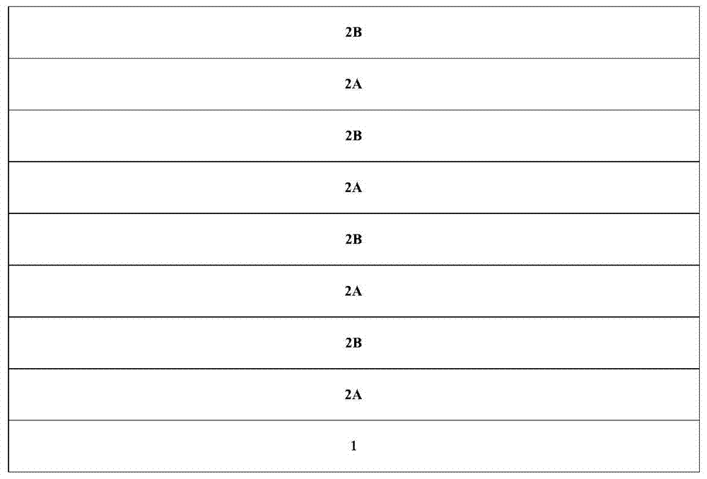
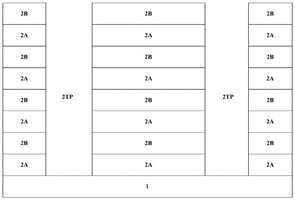
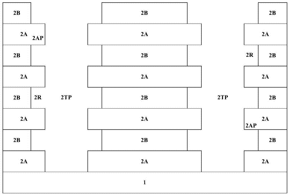
[0035] Such as figure 1 As shown, a stack structure 2 of first material layers 2A and second material layers 2B is alternately formed on a substrate 1 . The material of the substrate 1 may include bulk silicon (bulk Si), bulk germani...


PUM


Abstract

The invention discloses a three-dimensional semiconductor device, which comprises a plurality of storage units and a plurality of selection transistors, each of the plurality of storage units comprises: a channel layer distributed along a direction perpendicular to the surface of a substrate; a plurality of interlayers The insulating layer and multiple gate stack structures are alternately stacked along the sidewall of the channel layer; multiple floating gates are located between the multiple interlayer insulating layers and the sidewall of the channel layer; the drain a pole, located on the top of the channel layer; and a source, located in the substrate between two adjacent memory units of the plurality of memory units. According to the three-dimensional semiconductor device and its manufacturing method of the present invention, the floating gate is implanted on the sidewall of the vertical channel, and the opening of the source and drain regions induced on the sidewall of the vertical channel is controlled through the coupling between the gate electrode and the floating gate, effectively The induction efficiency and intensity of the source-drain region are improved, and the source-drain resistance of the storage unit is reduced, thereby increasing the reading current and the reading speed of the storage array.

Description

technical field [0001] The invention relates to a semiconductor device and a manufacturing method thereof, in particular to a three-dimensional semiconductor device and a manufacturing method thereof. Background technique [0002] In order to improve the density of memory devices, the industry has made extensive efforts to develop methods of reducing the size of two-dimensionally arranged memory cells. As the size of memory cells in two-dimensional (2D) memory devices continues to shrink, signal collisions and interference can increase significantly, making it difficult to perform multi-level cell (MLC) operations. In order to overcome the limitations of 2D memory devices, the industry has developed memory devices with a three-dimensional (3D) structure to increase integration density by three-dimensionally arranging memory cells on a substrate. [0003] Specifically, a multilayer stack structure (for example, a plurality of ONO structures alternating with oxides and nitrid...

Claims


Application Information

Patent Timeline
Patent Type & Authority Patents(China)
IPC IPC(8): H01L29/78H01L21/336H01L29/41
CPCH10B41/20H10B41/27H01L29/7889H01L29/7926H10B43/27H01L29/1037H01L29/7887
Inventor 霍宗亮
Owner INST OF MICROELECTRONICS CHINESE ACAD OF SCI
Why Eureka
Try Eureka