SiC secondary epitaxial structure

A secondary epitaxy and silicon carbide technology, which is applied in the direction of electrical components, circuits, semiconductor devices, etc., can solve the problems of crystallization quality decline, device processing technology without wet etching process, and low activation rate of implanted ions

Active Publication Date: 2012-02-08
THE 13TH RES INST OF CHINA ELECTRONICS TECH GRP CORP
View PDF0 Cites 0 Cited by
  • Summary
  • Abstract
  • Description
  • Claims
  • Application Information

AI Technical Summary

Problems solved by technology

[0004] 1. The depth of ion implantation in silicon carbide is shallow, the activation rate of implanted ions is very low, and the implantation efficiency is low, which makes it difficult to apply this common and important process in semiconductor preparation
[0005] 2. There is no practical wet etching process in the device processing technology, only dry etching process can be used
[0007] 1. Dry etching will cause damage, resulting in a decrease in carrier mobility that is critical to device performance, a decrease in crystal quality, and degradation of material properties, ultimately affecting device performance
[0008] 2. The length of the process flow is increased, resulting in a decrease in the final yield
[0009] 3. Increased equipment cost and process cost
Since the influence of thermal stress is reduced, and silicon carbide materials have very high thermal conductivity and good oxidation resistance, the thermal stability of devices using silicon carbide structures will be greatly improved. However, if unintentional Doped intrinsic silicon carbide layer, the source and drain of conventional MESFET (Metal Field Effect Transistor) devices are difficult to lead out

Method used


Image

  • SiC secondary epitaxial structure
  • SiC secondary epitaxial structure
  • SiC secondary epitaxial structure

Examples


Embodiment Construction

[0026] The present invention will be described in further detail below in conjunction with the accompanying drawings.

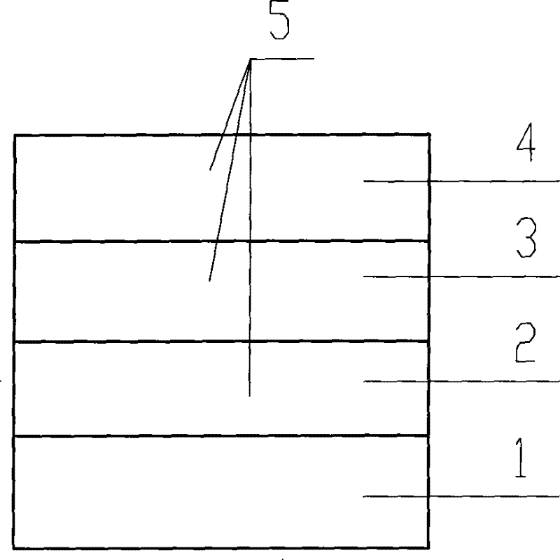
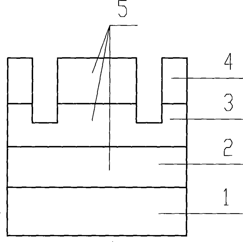
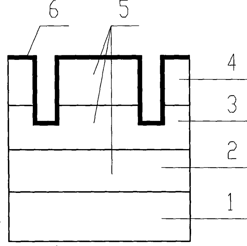
[0027] Such as Figure 1-3 As shown, the silicon carbide secondary epitaxial material structure used for the preparation of silicon carbide devices includes: a silicon carbide single crystal substrate 1, a primary homoepitaxial layer 5 formed on the surface of the silicon carbide single crystal substrate 1, and a primary homoepitaxial layer The secondary epitaxial layer 6 generated on the surface of 5, the secondary epitaxial layer 6 is formed after the primary homoepitaxial layer 5 is patterned and processed, wherein the primary homoepitaxial layer 5 includes p-type silicon carbide buffer layers 2, n Type silicon carbide active layer 3 and unintentionally doped intrinsic silicon carbide layer 4 .

[0028] The invention is applicable to the preparation of the ohmic contact of the source and drain parts of the silicon carbide MESFET device. In the specific i...


PUM


Abstract

The invention discloses a silicon carbide secondary epitaxial material structure used for the preparation of silicon carbide devices, comprising: a silicon carbide single crystal substrate, a primary homoepitaxial layer located on the surface of the substrate, and a primary homoepitaxial layer located on the surface of the primary homoepitaxial layer The secondary epitaxial layer, wherein the primary homoepitaxial layer includes a p-type silicon carbide buffer layer, an n-type silicon carbide active layer and an unintentionally doped intrinsic silicon carbide layer. Compared with the MESFET (Metal Field Effect Transistor) with a general structure, the MESFET prepared by the secondary epitaxial method has the advantages of small source-drain resistance, large ohmic contact area, and uniform electric field distribution in the working area of ​​the tube, which can improve transconductance. Increase the working voltage and power of the device. At the same time, the process of device preparation is greatly simplified and the stability of the device is guaranteed.

Description

technical field [0001] The invention relates to a silicon carbide secondary epitaxy structure, in particular to a silicon carbide secondary epitaxy structure which can shorten the process flow and improve the performance of silicon carbide devices. Background technique [0002] Silicon carbide material is one of the representative materials of the third-generation semiconductor. Compared with the first-generation semiconductor element material represented by silicon and the second-generation compound semiconductor material represented by gallium arsenide, silicon carbide has a wide band gap and high critical mass. Breakdown electric field, high carrier saturation drift velocity, high thermal conductivity and other characteristics. Specifically, taking 4H-SiC as an example, at 300K (27°C), the forbidden band width of silicon carbide is 3.2eV, which is much wider than 1.12eV of silicon and 1.43eV of gallium arsenide. In this way, the operating temperature of silicon carbide m...

Claims


Application Information

Patent Timeline
Patent Type & Authority Patents(China)
IPC IPC(8): H01L29/24H01L21/336
Inventor 杨霏潘宏菽陈昊冯震吕云安齐国虎张志国冯志红蔡树军杨克武
Owner THE 13TH RES INST OF CHINA ELECTRONICS TECH GRP CORP
Why Eureka
Try Eureka