Manufacturing method of silicon MOS transistor on partially consumed insulating layer

A MOS transistor, silicon-on-insulator technology, applied in semiconductor/solid-state device manufacturing, electrical components, circuits, etc., can solve the problems of difficult integration of PDSOIMOS transistors, limited gate-to-channel control capability, and reduced threshold voltage, etc. Achieve the effect of enhancing the ability to resist short channel effects, suppressing the drain-induced barrier lowering effect, and reducing the impurity compensation effect

Inactive Publication Date: 2011-09-07
PEKING UNIV SHENZHEN GRADUATE SCHOOL
View PDF0 Cites 5 Cited by
  • Summary
  • Abstract
  • Description
  • Claims
  • Application Information

AI Technical Summary

Problems solved by technology

However, in the prior art, due to the limited control ability of the gate to the channel of the PD SOI MOS transistor, the short-channel effect is serious, and the short-channel effect reduces the threshold voltage, and at the same time leads to the punch-through in the source-drain region, so the PD SOIMOS transistors are also difficult to apply to the production of integrated circuits at the nanoscale

Method used


Image

  • Manufacturing method of silicon MOS transistor on partially consumed insulating layer
  • Manufacturing method of silicon MOS transistor on partially consumed insulating layer
  • Manufacturing method of silicon MOS transistor on partially consumed insulating layer

Examples


Embodiment Construction

[0030] The present invention will be described in further detail below with specific embodiments in conjunction with the accompanying drawings.

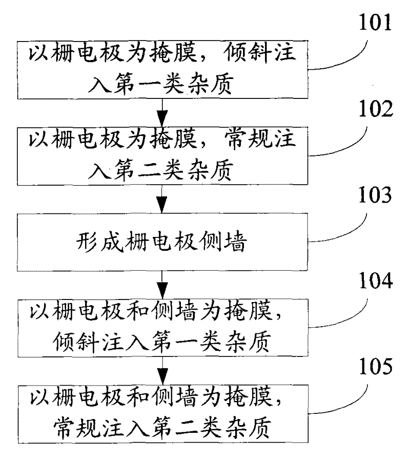
[0031] The present invention utilizes the structure of SOI silicon wafer, and through the design of the manufacturing process, when the body region of the PD SOI MOS transistor is doped, a heavily doped region is formed in the channel region, while no heavily doped region is formed in the source and drain regions. In order to maximize the channel effect of the control terminal, at the same time, it does not obviously bring various parasitic effects. In order to make the heavily doped region exhibit the above-mentioned distribution, the present invention adopts a two-time inclined ion implantation method combined with a reasonable combination of implantation energy and dose to implant a certain amount of impurities.

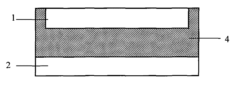
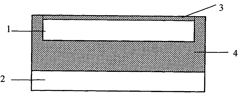
[0032] The structure of SOI wafer is as figure 1 As shown, it includes a bulk silicon substrate 2 , a buried oxide la...


PUM


Abstract

The invention discloses a manufacturing method of a PD SOI MOS transistor, which comprises the processes of defining an active area on an SOI silicon chip and doping after a gate electrode is formed, wherein the processes comprise the steps of: A. implanting angled ions by taking the gate electrode as a masking film, wherein the type of the implanted impurity is a first type of impurity with the same type as that of the impurity at the bottom inside the silicon film layer of the SOI silicon chip; B. implanting conventional ions by taking the gate electrode as the masking film, wherein the type of the implanted impurity is a second type of impurity with the type opposite to that of the first type of impurity; C. forming side wall layers at two sides of the gate electrode; D. implanting theangled ions by taking the gate electrode and the side wall layers as the masking film, wherein the type of the implanted impurity is the first type of impurity, and the ion implantation energy is setto be higher than that of the angled ions in step A; and E, implanting the conventional ions by taking the gate electrode and the side wall layers as the masking film, wherein the type of the implanted impurity is the second type of impurity. The method effectively inhibits the punch-through of DIBL effect and source leakage deep areas, thus greatly promoting the short channel effect resistant capability of the device.

Description

technical field [0001] The invention relates to the technical field of semiconductor integrated circuits and its manufacture, in particular to a method for manufacturing SOIMOS transistors. Background technique [0002] The main device of an integrated circuit, especially a VLSI, is a MOS transistor (MetalOxide Semiconductor Field Effect Transistor, Metal-Oxide-Semiconductor Field Effect Transistor, MOSFET for short). Since the invention of the MOS transistor, it has made rapid progress in performance and function, and this progress has been achieved largely by continuously reducing the size of the device and increasing the chip area. The shrinking of device size leads to the continuous improvement of circuit performance, the continuous increase of circuit density, and the expansion of chip size also promotes the continuous increase of circuit functions. As the geometries of MOSFETs continue to shrink, now with feature sizes at the nanoscale, various practical and fundament...

Claims


Application Information

Patent Timeline
Patent Type & Authority Patents(China)
IPC IPC(8): H01L21/336H01L21/266
Inventor 张盛东廖聪维韩汝琦
Owner PEKING UNIV SHENZHEN GRADUATE SCHOOL
Why Eureka
Try Eureka