Step-by-step projection photo-etching machine double set shifting exposure ultra-sophisticated positioning silicon chip bench system

A silicon wafer stage, projection light technology, applied in microlithography exposure equipment, photolithography process exposure devices, optics, etc., can solve the problems of system positioning accuracy, system complexity, double-stage collision, etc., and reduce adverse effects. , the effect of improving exposure efficiency and reducing complexity

Active Publication Date: 2004-03-31
SHANGHAI MICRO ELECTRONICS EQUIP (GRP) CO LTD +1
View PDF3 Cites 58 Cited by
  • Summary
  • Abstract
  • Description
  • Claims
  • Application Information

AI Technical Summary

Problems solved by technology

The main difference between the two is that the scanning lithography machine has a mask motion positioning system that can perform large-scale scanning motion positioning, while the stepping lithography machine does not
[0008] However, there are still some problems in this dual-stage structure: first, when the two wafer stages are exchanged, the two silicon wafer stages will be in a free state for a short period of time, which will undoubtedly have a certain impact on the positioning accuracy of the system , and to solve this problem would compl

Method used


Image

  • Step-by-step projection photo-etching machine double set shifting exposure ultra-sophisticated positioning silicon chip bench system
  • Step-by-step projection photo-etching machine double set shifting exposure ultra-sophisticated positioning silicon chip bench system
  • Step-by-step projection photo-etching machine double set shifting exposure ultra-sophisticated positioning silicon chip bench system

Examples


Embodiment Construction

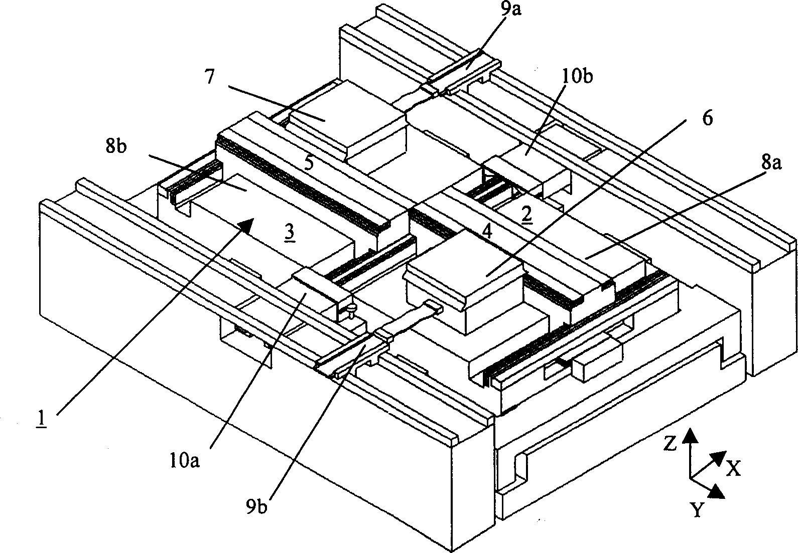
[0052] figure 2 Shows the status of the entire system at work. At this time, the double-sided buttable linear guide rails 4, 5 and the silicon wafer carrying device 6, 7 complete the set action at the exposure station and the silicon wafer pretreatment station respectively, and the bridging devices 10a, 10b are in the non-bridging position and will not Interference with the Linear Way unit. The cable tables 9a, 9b are driven by their driving devices, so that the cables on the silicon wafer carrying device keep moving synchronously with the silicon wafer carrying device.

[0053] image 3 It shows the situation when the system is working in the switching state. First, the double-sided buttable linear guide units 4, 5 and the wafer carrying devices 6, 7 enter the exchange position P together. 1 ,P 2 , at this moment, the double-sided linear guide rails 4, 5 are accurately docked. Then the bridging device is driven by its driving device to move toward each other along the ...


PUM


Abstract

A step-by-step projection photo-etching machine double shift exposure ultra precise positioning silicon chip bench system, comprising a silicon chip bench positioning unit operating in the exposure station, and a silicon chip bench positioning unit operating in the preliminary treatment station, each positioning unit includes a silicon chip carrying device. The system can increase the exposure efficiency without the problem of overlapping and interference in the working space. It also realizes simplified structure, and high reliability and positioning precision.

Description

technical field [0001] The invention relates to an ultra-precise motion positioning system for silicon wafers in the photoetching process. The system can be used for both scanning photoetching machines and stepping photoetching machines. Background technique [0002] In the production process of integrated circuit chips, the exposure transfer (photolithography) of the design pattern of the chip on the photoresist on the surface of the silicon wafer is one of the most important processes. The equipment used in this process is called a photolithography machine (exposure machine). The resolution and exposure efficiency of the lithography machine greatly affect the characteristic line width (resolution) and productivity of the integrated circuit chip. As the main component of the lithography machine, the motion accuracy and work efficiency of the silicon wafer ultra-precision motion positioning system determine the resolution and exposure efficiency of the lithography machine t...

Claims


Application Information

Patent Timeline
IPC IPC(8): F16C32/06G03F7/20G03F9/00H01L21/027H01L21/68
Inventor 汪劲松朱煜张鸣尹文生段广洪杨学智徐登峰杨开明朱立伟王建发于晖
Owner SHANGHAI MICRO ELECTRONICS EQUIP (GRP) CO LTD
Why Eureka
Try Eureka