Semiconductor device and method for manufacturing the same

a technology of semiconductor devices and semiconductors, applied in semiconductor devices, semiconductor/solid-state device details, electrical apparatus, etc., can solve the problems of increasing the contact resistance between bumps, and less productive, so as to reduce the possibility of void generation

Inactive Publication Date: 2012-03-22
HITACHI LTD
View PDF7 Cites 58 Cited by
  • Summary
  • Abstract
  • Description
  • Claims
  • Application Information

AI Technical Summary

Benefits of technology

[0022]The advantageous effects achieved by the preferred embodiments of the present invention as disclosed herein are briefly summarized below.
[0023]According to the first aspect of the invention, a cavity is made on the junction surface between the first and second substrates due to the recess in the surface of the first conductive film buried in the first channel. This allows the air trapped on the junction surface to get out through the cavity, thereby reducing the possibility of generation of voids.
[0024]According to the second aspect of the invention, when the semiconductor substrate and another substrate are bonded with one surface of the semiconductor substrate facing one surface of the other substrate, a cavity is made on the junction surface between the substrates due to the recess in the surface of the first conductive film buried in the first channel of the semiconductor substrate. This allows the air trapped on the junction surface to get out through the cavity, thereby reducing the possibility of generation of voids.

Problems solved by technology

Consequently the bumps would corrode because they contact with the chemical solution, resulting in an increase in the contact resistance between bumps.
In addition, the air trapped in the channels might cause oxidization of the bump surface, resulting in a further increase in the contact resistance between bumps.
Since this process involves a number of steps, it is less productive.

Method used


Image

  • Semiconductor device and method for manufacturing the same
  • Semiconductor device and method for manufacturing the same
  • Semiconductor device and method for manufacturing the same

Examples


Embodiment Construction

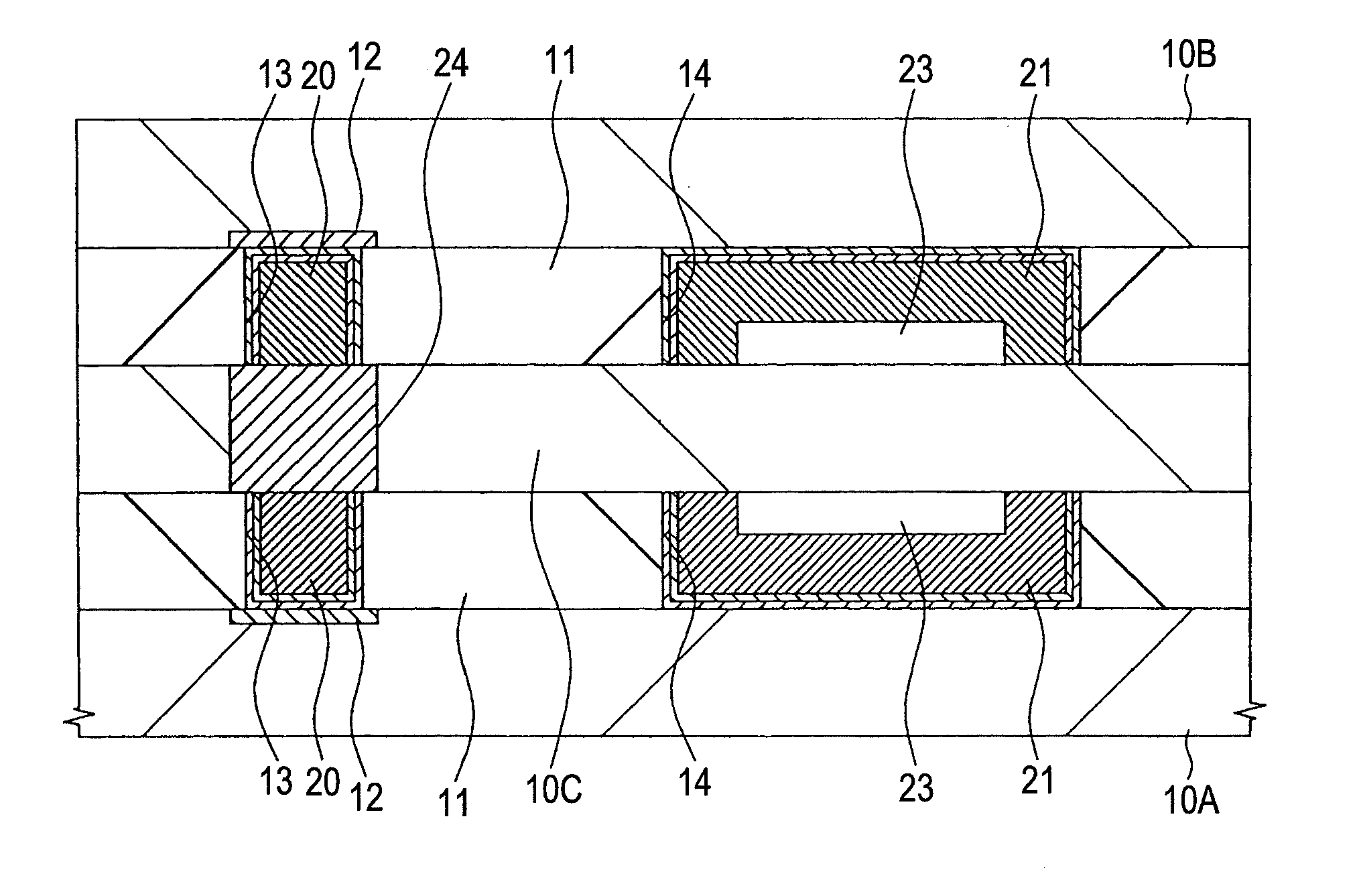
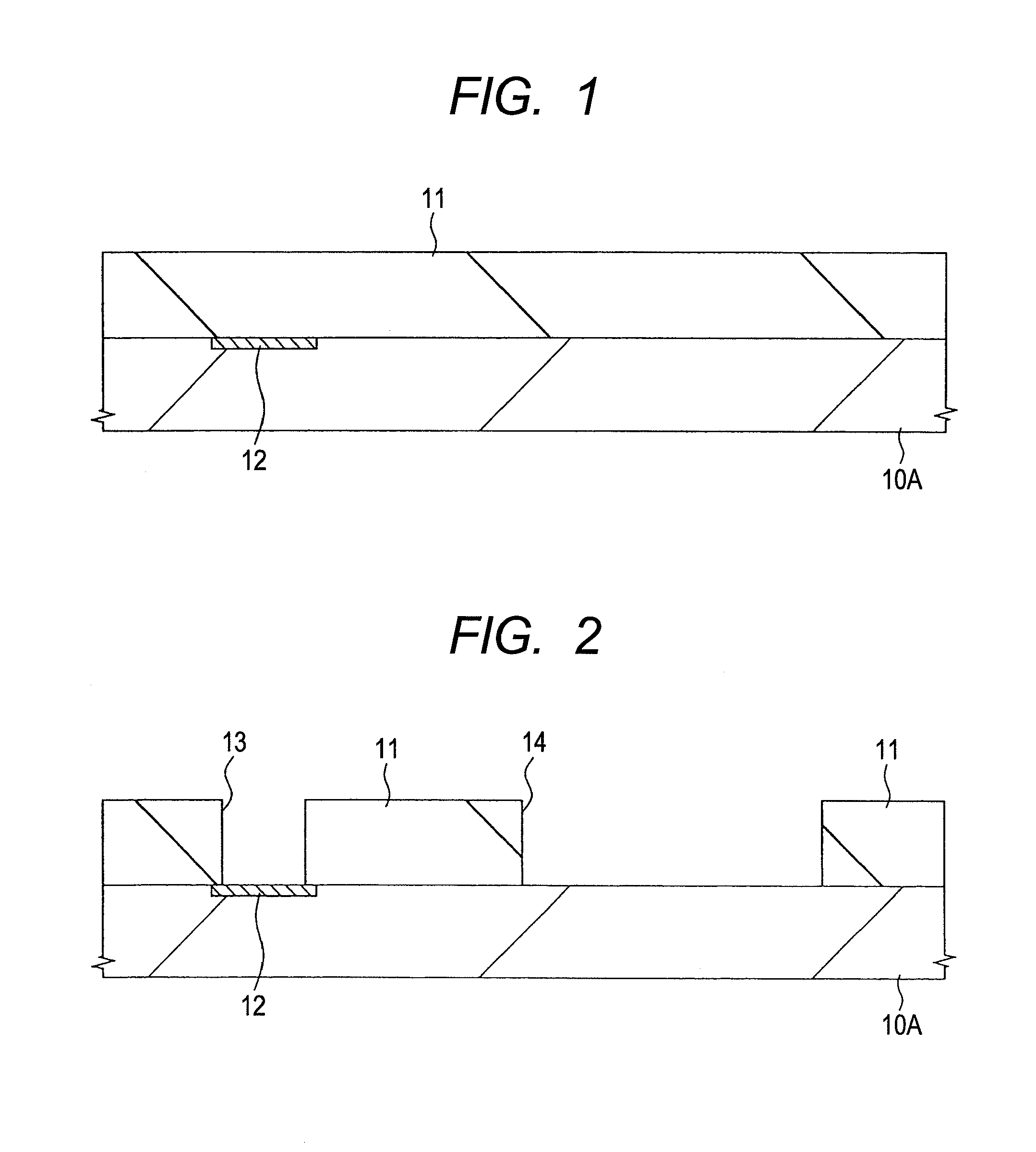
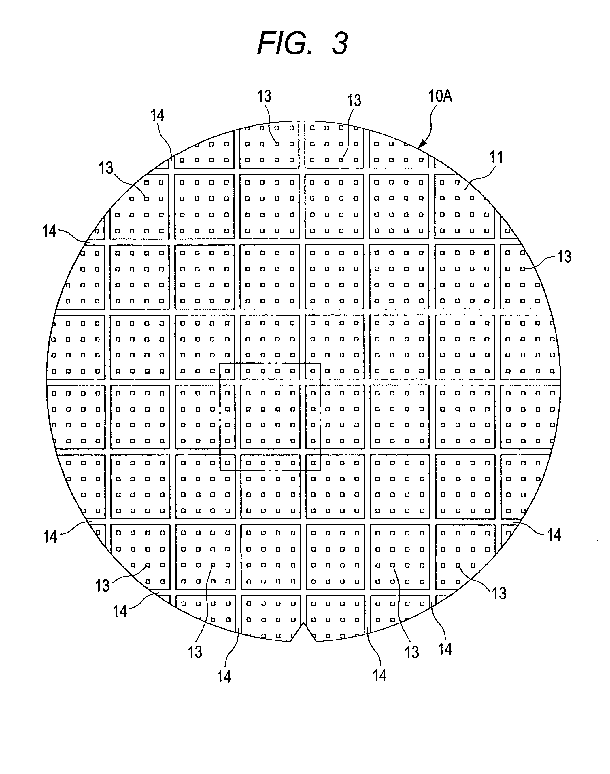
[0048]Next, the preferred embodiments of the present invention will be described in detail referring to the accompanying drawings. In all the drawings that illustrate the preferred embodiments, elements with like functions are designated by like reference numerals and repeated descriptions of such elements are omitted. Descriptions of same or similar elements in the preferred embodiments are basically not repeated. In drawings that illustrate a preferred embodiment, hatching may be used even in a plan view for easy understanding or hatching may be omitted even in a sectional view.

[0049]The semiconductor device according to a first embodiment of the invention is a stack semiconductor device in which two silicon wafers with multiple bumps and a resin film surrounding them formed on their main surfaces are bonded together and the integrated circuits formed on the silicon wafers are electrically coupled through bumps.

[0050]Next, a method for manufacturing the semiconductor device accord...


PUM


Abstract

A semiconductor device including two silicon wafers stacked and bonded together with bumps of one wafer electrically coupled with those of the other wafer, in which generation of voids on the junction surface between the silicon wafers is suppressed. Due to a recess made in the surface of a buried conductive film, a cavity is formed in the junction surface between the silicon wafers. The ends of the cavity extend to the periphery of the junction surface between the silicon wafers. This allows the air trapped on the junction surface between the silicon wafers to get out through the cavity, thereby reducing the possibility of generation of voids on the junction surface.

Description

CLAIM OF PRIORITY[0001]The present application claims priority from Japanese patent application JP 2010-211078 filed on Sep. 21, 2010, the content of which is hereby incorporated by reference into this application.FIELD OF THE INVENTION[0002]The present invention relates to a semiconductor device and a method for manufacturing the same and more particularly to technology for a semiconductor device including multiple semiconductor substrates electrically coupled through bumps and the manufacture thereof.BACKGROUND OF THE INVENTION[0003]In recent years, as an approach to reducing the size of a semiconductor device and enhancing its performance, packaging techniques that semiconductor substrates of single-crystal silicon (hereinafter called silicon substrates) are stacked and electrically coupled using microelectrode wires have been developed.[0004]Among these packaging techniques, a technique which has been recently attracting attention is that the integrated circuits formed on plural...

Claims


Application Information

Patent Timeline
Patent Type & Authority Applications(United States)
IPC IPC(8): H01L23/48H01L21/28
CPCH01L23/481H01L2924/10253H01L25/50H01L2225/06513H01L2224/13687H01L2224/13565H01L2224/26122H01L2224/11602H01L23/562H01L24/13H01L24/29H01L24/81H01L24/83H01L24/92H01L2224/11462H01L2224/1148H01L2224/13019H01L2224/13147H01L2224/13582H01L2224/13647H01L2224/1403H01L2224/14051H01L2224/2919H01L2224/73104H01L2224/81007H01L2224/81203H01L2224/83007H01L2224/83203H01L2224/83862H01L2224/9211H01L2224/94H01L2924/00013H01L2924/01029H01L25/0657H01L2224/11H01L2924/00014H01L2924/04941H01L2224/81H01L2224/83H01L2224/13099H01L2224/05099H01L2224/13599H01L2224/05599H01L2224/29099H01L2224/29599H01L2924/00H01L24/05H01L24/08H01L24/09H01L24/80H01L2224/0401H01L2224/05547H01L2224/05551H01L2224/05557H01L2224/05571H01L2224/0603H01L2224/06051H01L2224/0807H01L2224/08111H01L2224/08121H01L2224/09515H01L2224/80357H01L2224/80894H01L2924/14H01L2924/00012
Inventor AOKI, MAYUTAKEDA, KENICHIHOZAWA, KAZUYUKI
Owner HITACHI LTD
Why Eureka
Try Eureka