Ion beam sputtering apparatus and film deposition method for a multilayer for a reflective-type mask blank for EUV lithography

a technology of euv lithography and ion beam sputtering apparatus, which is applied in the direction of photomechanical treatment originals, instruments, nanoinformatics, etc., can solve the problems of deterioration of the characteristics of the film to be formed, close limit of light exposure exposure, and degradation of the quality of the film, so as to reduce the possibility of generating particles at the inner wall of the chamber or another ion sour

Inactive Publication Date: 2007-04-19
ASAHI GLASS CO LTD
View PDF7 Cites 18 Cited by
  • Summary
  • Abstract
  • Description
  • Claims
  • Application Information

AI Technical Summary

Benefits of technology

[0026] According to the first film deposition method of the present invention, particles from an inner wall or the like of the chamber can be prevented from reaching the substrate during film formation. According to the first film deposition method of the present invention, a high-quality reflective-type mask blank for EUV lithography wherein there is no impermissible defect, specifically, a defect of 30 nm or larger in the multilayer film including a reflective layer and a protective layer formed thereon is at most 0.05 number / cm2, particularly, at most 0.005 number / cm2, can be produced.
[0027] The first ion beam sputtering apparatus of the present invention is suited for carrying out the above-mentioned first film deposition method of the present invention.
[0028] According to the second film deposition method of the present invention, the particles generated at the ion source can also be presented from reaching the substrate during film formation, whereby a high-quality reflective-type mask blank for EUV lithography wherein there is no impermissible defect, specifically, a defect of 30 nm or larger in the multilayer film including a reflective layer and a protective layer formed thereon is at most 0.005 number / cm2, can be produced.
[0029] The second ion beam sputtering apparatus of the present invention is suited for carrying out the above-mentioned second film deposition method of the present invention.
[0030] In the third film deposition method of the present invention, ion beams from the ion source are deflected to be injected into the sputtering target. Accordingly, even in a case of using a plurality of ion sources disposed at symmetrical positions, the possibility that the atoms sputtered by ion beams move toward another ion source, can be reduced. With such measures, it is possible to reduce the possibility of generating particles at the ion source.
[0031] Further, when ion beams are deflected to be injected into the sputtering target in a vertical direction, almost the sputtered atoms move toward the film deposition substrate, and the movement in another direction, specifically, the direction of an inner wall of the chamber or another ion source can be minimized. As a result, generation of particles at the inner wall of the chamber or another ion source can remarkably be reduced.

Problems solved by technology

However, the conventional exposure techniques using light exposure have been close to the limit while semiconductor devices have had finer patterns at an accelerated pace.
Since these bouncing ions reach the substrate at a high speed without losing a sufficient amount of kinetic energy that the ions possess originally, they sputter the film material deposited on the substrate or roughen the film surface when they enter into the substrate, whereby the characteristics of the film to be formed become deteriorated.
Thus, the conventional method caused degradation in the quality of the film.
However, in the view of the system principle that the atoms of the material constituting the target are sputtered by ions entering into the target, it is practically impossible to lead all the sputtered atoms to an intended direction, specifically toward the substrate.
If particles of the deposited films separated from the inner wall or the like enter into films being deposited, the mask blank to be manufactured has defects.
In the conventional ion beam sputtering apparatuses, the defect caused by the mixing of particles in a film being deposited was immaterial in comparison with the deterioration of the film quality caused by bouncing ions.
However, in the case of a reflective-type mask blank for EUV lithography, such minor defect becomes problematic.
However, it was impossible for the conventional ion beam sputtering apparatuses to reduce the defect to such a level.
When the particles generated at the ion source enter into the film being deposited, the mask blank has defects.

Method used


Image

  • Ion beam sputtering apparatus and film deposition method for a multilayer for a reflective-type mask blank for EUV lithography
  • Ion beam sputtering apparatus and film deposition method for a multilayer for a reflective-type mask blank for EUV lithography
  • Ion beam sputtering apparatus and film deposition method for a multilayer for a reflective-type mask blank for EUV lithography

Examples


first embodiment

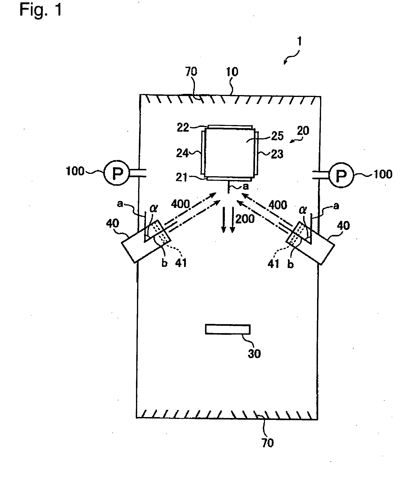
[0057] In the following, description will be made further on the present invention with reference to figures. FIG. 1 is a schematic view showing an ion beam sputtering apparatus (the first ion beam sputtering apparatus of the present invention) usable when the film deposition method of the present invention is employed. In the ion beam sputtering apparatus 1 shown in FIG. 1, a chamber 10 is provided with a vacuuming device (vacuum pump) 100 by which the inside of the chamber can be maintained in a vacuumed state. In the chamber 10, a sputtering target 21 and a substrate on which a film is deposited (hereinbelow, referred possible to as the substrate) 30 are disposed facing each other with a predetermined space. On wall surfaces of the chamber 10, two ion sources 40 are disposed at positions to be symmetric laterally in the figure. Each ion source 40 discharges ions extracted from plasma, as ion beams 400. The ion beams 400 from the ion source 40 enter obliquely into the sputtering t...

second embodiment

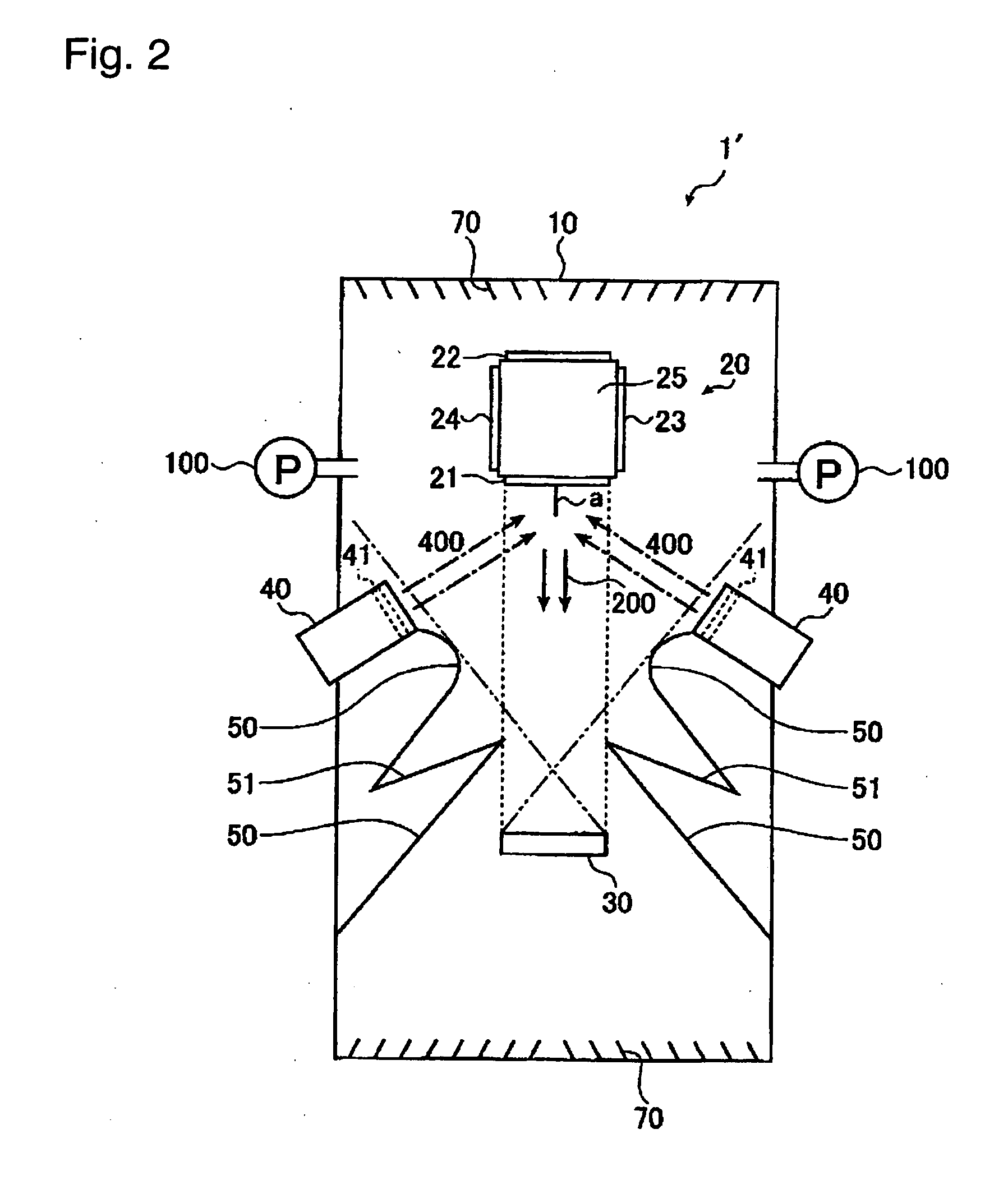
[0071]FIG. 2 is a schematic view showing an ion beam sputtering apparatus (the second ion beam sputtering apparatus) usable when the film deposition method of the present invention is employed. In FIG. 2, the same reference numerals as in FIG. 1 are used in the same meaning as in FIG. 1.

[0072] In the second embodiment of the film deposition method of the present invention (hereinbelow, referred to as “the second film deposition method of the present invention”) is characterized in that ion beams are injected to a sputtering target from an ion source which is disposed at a position out of the region where particles move linearly from a film deposition substrate toward the sputtering target.

[0073] In the ion beam sputtering apparatus 1′ in FIG. 2, a device useful for carrying out the second film deposition method of the present invention is shown. Specifically, baffle plates 50 are attached to the inner walls of the chamber 10 from the locations where the ion sources 40 are disposed,...

third embodiment

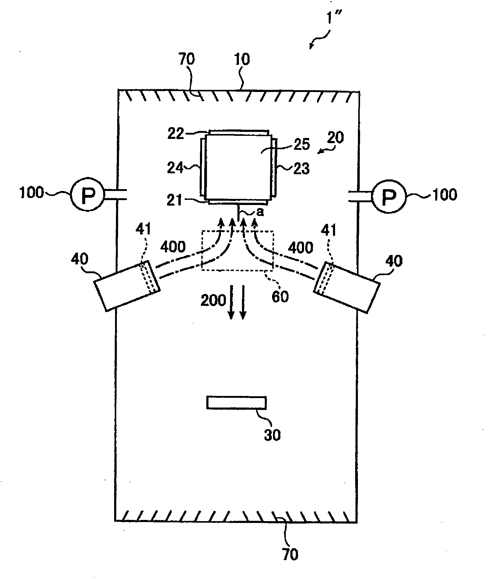
[0078]FIG. 3 is a schematic view showing an ion beam sputtering apparatus (the third ion beam sputtering apparatus) usable for the film deposition method of the present invention. In FIG. 3, the same reference numerals as in FIG. 1 are used in the same meaning as in FIG. 1.

[0079] The third embodiment of the film deposition method of the present invention (hereinbelow, referred to as “the third film deposition method of the present invention”) is characterized in that ion beams from an ion source are deflected by the action of a magnetic field to be injected into the sputtering target.

[0080] The ion beam sputtering apparatus 1″ shown in FIG. 3 is provided with a device for carrying out the second film deposition method of the present invention.

[0081] The ion beam sputtering apparatus 1″ shown in FIG. 3 has a device 60 for deflecting ion beams 400 (ion beam deflecting device) from an ion source 40 by the action of a magnetic field. The ion beams 400 from the ion source 40 is deflect...


PUM

PropertyMeasurementUnit
relative distanceaaaaaaaaaa
temperatureaaaaaaaaaa
wavelengthaaaaaaaaaa

Abstract

A film deposition method for a multilayer for a EUV mask blank by which a defect caused by the mixing of a particle in the layer during film formation can be prevented and an ion beam sputtering apparatus suitable for the method are presented. A film deposition method for forming a multilayer for a reflective-type mask blank for EUV lithography on a film deposition substrate by using an ion beam sputtering method, the film deposition method being characterized in that a sputtering target and a film deposition substrate are disposed at opposed positions with a predetermined space, and ion beams are injected to the sputtering target from an ion source which is disposed at a position out of the region where particles move linearly from the film deposition substrate toward the sputtering target.

Description

TECHNICAL FIELD [0001] The present invention relates to an ion beam sputtering apparatus suitable for forming a multilayer for a reflective-type mask blank for EUV (extreme ultraviolet) lithography and a method for depositing a multilayer for a reflective-type mask blank for EUV lithography by using an ion beam sputtering method. BACKGROUND ART [0002] In the semiconductor industry, a photolithography method using visible light or ultraviolet light has been employed as a technique for writing, on a Si substrate or the like, a fine pattern, which is required for writing an integrated circuit comprising such a fine pattern. However, the conventional exposure techniques using light exposure have been close to the limit while semiconductor devices have had finer patterns at an accelerated pace. In the case of light exposure, it is said that the resolution limit is about ½of exposure wavelength, and even if an F2 laser (157 nm) is employed, it is estimated that the resolution limit of a p...

Claims


Application Information

Patent Timeline
Patent Type & Authority Applications(United States)
IPC IPC(8): H01L21/31H01L21/469G03F1/24
CPCB82Y10/00B82Y40/00C23C14/46G03F1/24C23C14/34
Inventor SUGIYAMA, TAKASHIUNO, TOSHIYUKITAKAKI, SATORU
Owner ASAHI GLASS CO LTD
Why Eureka
Try Eureka