AI technical title is built by PatSnap AI team. It summarizes the technical point description of the patent document.
a bonding structure and pillar technology, applied in the direction of electrical equipment, semiconductor devices, semiconductor/solid-state device details, etc., can solve the problems of low overall yield of the flip-chip package, bad electrical connection etc., to reduce the separation between neighboring bonding pads, improve the reliability of the junction and increase the separation distance between the chip and the substrate.
Inactive Publication Date: 2007-04-24
QUALCOMM INC
View PDF13 Cites 60 Cited by
Summary
Abstract
Description
Claims
Application Information
AI Technical Summary
This helps you quickly interpret patents by identifying the three key elements:
Problems solved by technology
Method used
Benefits of technology
Benefits of technology
[0012]Accordingly, one object of the present invention is to provide a cylindrical bonding structure and its method of manufacture capable of reducing the separation between neighboring bonding pads on a chip while increasing distance of separation between the chip and a substrate. Ultimately, reliability of the junctions connecting the chip and the substrate is improved and post-packaging life of the chip is extended.
[0013]A second object of this invention is to provide a cylindrical bonding structure and its method of manufacture capable of reducing the diameter of openings on a solder mask for exposing a pad so that distance of separation between neighboring pads on the substrate is reduced. Consequently, the distance of separation between neighboring bonding pads (bumps) on the chip is also reduced.
[0014]A third object of this invention is to provide a cylindrical bonding structure and its method of manufacture that requires no application of low melting point solder material on the pads of a substrate or the surface of bumps before conducting a heat treating process. Thus, production cost of a flip-chip package is reduced.
Problems solved by technology
Poor adhesion often leads to bad electrical connections between the chip and the substrate and a low overall yield of the flip chip package.
Method used
Image
Click on the blue label to locate the original text in one second.
Reading with bidirectional positioning of images and text.
Examples
first embodiment
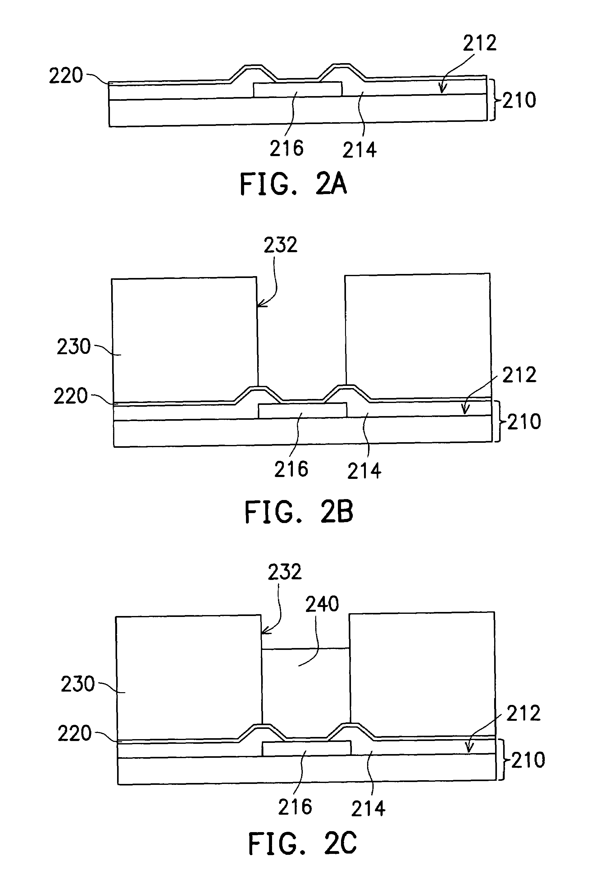
[0030]FIGS. 2A˜2F are schematic cross-sectional views showing the progression of steps for producing a cylindrical bonding structure according to this invention. As shown in FIG. 2A, a silicon wafer 210 is provided. Since each chip (not shown) is formed by cutting up the wafer 210 and any redistribution layer or bumps are formed before cutting, the wafer 210 actually represents a congregation of uncut chips. Furthermore, the active surface 212 of the wafer 210 has a passivation layer 214 and a plurality of bonding pads 216 (only one bonding pad is shown in FIG. 2A). The active surface 212 of the wafer 210 refers to the side of the wafer 210 where active devices are formed. The patterned passivation layer 214 exposes the bonding pads 216. Note that bonding pads 216 includes those original pads on the chips or the bonding pads of any redistribution circuit layer on the chips. The purpose of having a redistribution layer is to relocate the original bonding pads on the chip to some othe...
third embodiment
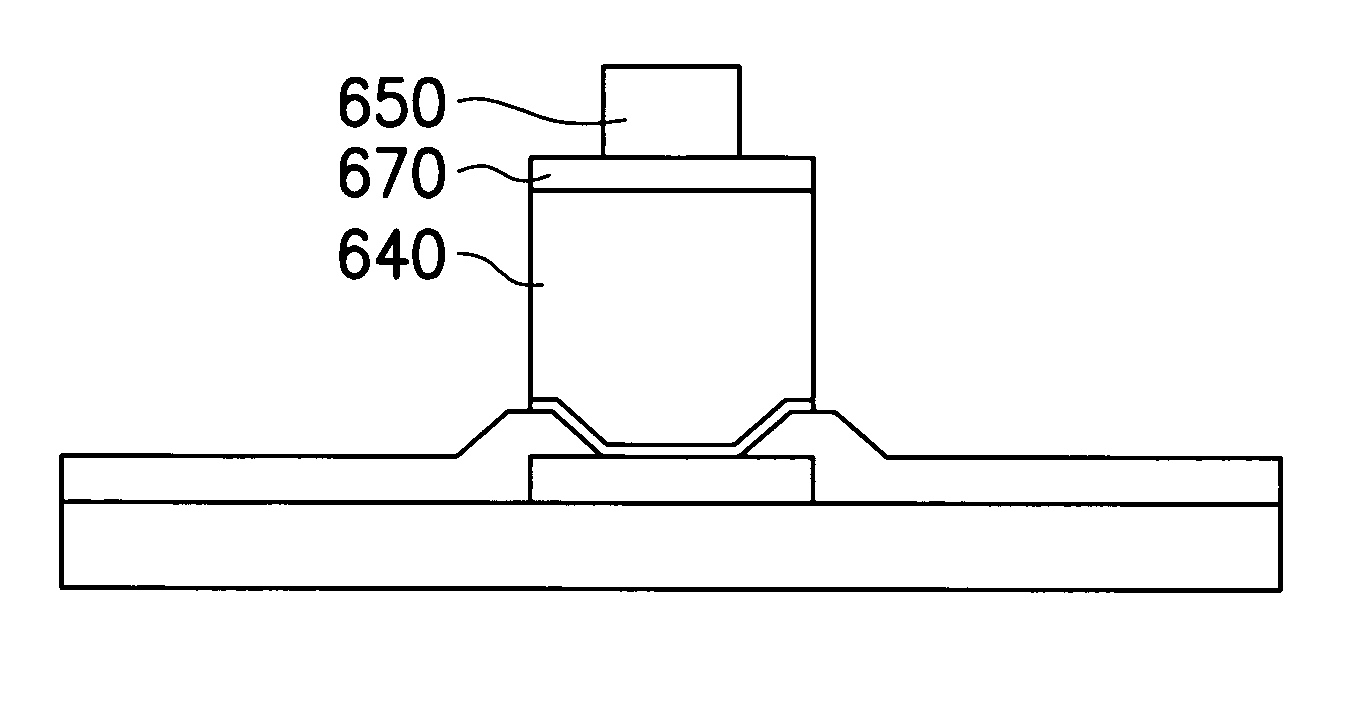
[0050]FIGS. 5A˜5C are schematic cross-sectional views showing an application of the third cylindrical bonding structure according to this invention to the fabrication of a flip-chip package. As shown in FIG. 5A, a cylindrical bonding structure 514 according to this invention is formed on the bonding pad 512 of a chip 510. The cylindrical bonding structure 514 comprises a ball contact metallic layer 514a, a conductive pillar 514b and a cylindrical solder cap 514c. In addition, a substrate 520 having a solder mask layer 524 and a pad 522 thereon is also provided. The solder mask 524 has a plurality of openings 526 that exposes the pads 522. In one aspect, the solder cap 514c has a transverse length w1 smaller than the corresponding transverse length w2 of the opening 526 in the solder mask layer 524 of the substrate 520. In one aspect, the solder cap 514c has a length D1 greater than the corresponding depth D2 of the opening 526 in the solder mask layer 524 of the substrate 520.
[0051]...
PUM
Abstract
A cylindrical bonding structure and its method of manufacture. The cylindrical bonding structure is formed over the bonding pad of a silicon chip and the chip is flipped over to connect with a substrate board in the process of forming a flip-chip package. The cylindrical bonding structure mainly includes a conductive pillar and a solder cap. The conductive pillar is formed over the bonding pad of the silicon chip and the solder cap is attached to the upper end of the conductive pillar. The solder cap has a melting point lower than the conductive pillar. The solder cap can be configured into a cylindrical, spherical or hemispherical shape. To fabricate the cylindrical bonding structure, a patterned mask layer having a plurality of openings that correspond in position to the bonding pads on the wafer is formed over a silicon wafer. Conductive material is deposited into the openings to form conductive pillars and finally a solder cap is attached to the end of each conductive pillar.
Description
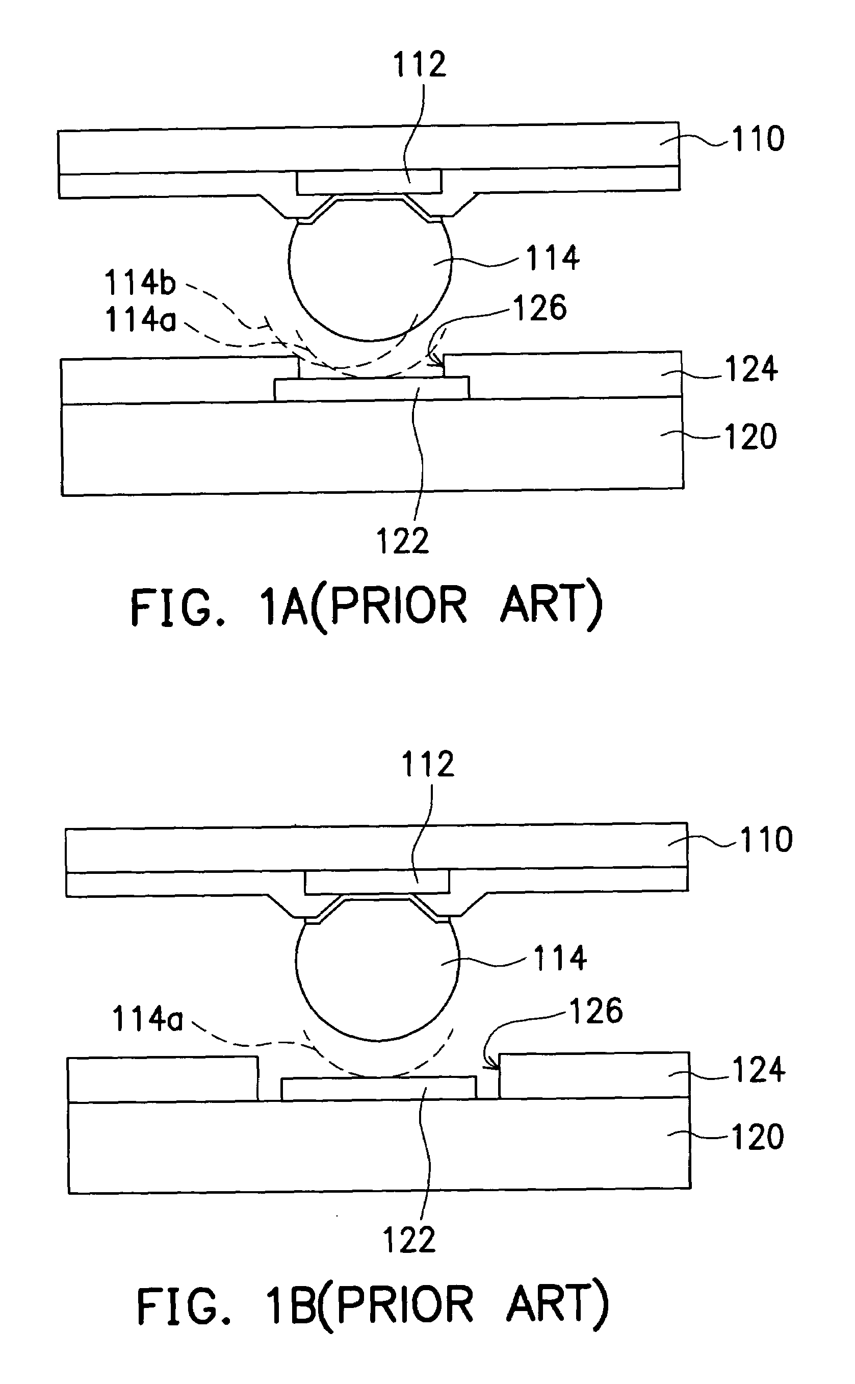
CROSS-REFERENCE TO RELATED APPLICATION[0001]This application is related to application Ser. No. 09 / 798,654 filed on Mar. 5, 2001, now U.S. Pat. No. 6,818,545; and related to application Ser. No. 10 / 935,451 filed on Sep. 7, 2004, now pending; and related to application Ser. No. 09 / 953,525 filed on Sep. 17, 2001, now U.S. Pat. No. 6,442,136; and related to application Ser. No. 10 / 638,454 filed on Aug. 11, 2003, now U.S. Pat. No. 6,917,119; and related to application Ser. No. 11 / 120,234 filed on May 2, 2005, now pending; and related to application Ser. No. 09 / 837,007 filed on Apr. 18, 2001, now pending; and related to application Ser. No. 10 / 055,580 filed on Jan. 22, 2002, now pending; and related to application Ser. No. 10 / 174,357 filed on Jun. 17, 2002, now U.S. Pat. No. 6,784,087; and related to application Ser. No. 10 / 695,630 filed on Oct. 27, 2003, now pending; and related to application Ser. No. 11 / 123,328 filed on May 6, 2005, now pending, all assigned to a common assignee.BACKG...
Claims
Application Information
Patent Timeline
Application Date:The date an application was filed.
Publication Date:The date a patent or application was officially published.
First Publication Date:The earliest publication date of a patent with the same application number.
Issue Date:Publication date of the patent grant document.
PCT Entry Date:The Entry date of PCT National Phase.
Estimated Expiry Date:The statutory expiry date of a patent right according to the Patent Law, and it is the longest term of protection that the patent right can achieve without the termination of the patent right due to other reasons(Term extension factor has been taken into account ).
Invalid Date:Actual expiry date is based on effective date or publication date of legal transaction data of invalid patent.

