Magnetoresistance effect element and magnetoresistive device

a technology of magnetoresistance and effect, which is applied in the field of magnetoresistance effect element and magnetoresistance device, can solve the problems of forming pin holes, etc., reducing the incidence rate of problems causing the breakdown of elements, increasing the number of broken down voltages, etc., and achieves high reproduction sensitivity, high quality, and high magnetoresistance effect

Inactive Publication Date: 2009-03-26
FUJITSU LTD +1
View PDF7 Cites 7 Cited by
  • Summary
  • Abstract
  • Description
  • Claims
  • Application Information

AI Technical Summary

Benefits of technology

[0026]The magnetoresistive device of the present invention includes the above described magnetoresistance effect element.
[0027]In the magnetoresistive device, the magnetoresistance effect element having the barrier layer is employed, so that very a high magnetoresistance effect can be obtained without deteriorating performance of the barrier layer. Therefore, a high quality magnetoresistive device, e.g., magnetic head with high reproduction sensitivity corresponding to high recording density, MRAM having improved storage property, can be provided.
[0028]For example, the magnetoresistance effect element of the present invention can be suitably applied to a data storage unit comprising: a head slider including a magnetoresistance element for reading data recorded on a recording medium, wherein the magnetoresistance effect element comprises a free layer, a pinned magnetic layer, and a barrier layer being provided between the free layer and the pinned magnetic layer and composed of a semiconductor; a suspension supporting the head slider; an actuator arm being capable of turning, wherein an end of the suspension is fixed to the actuator arm; and a signal detection circuit for detecting electric signals for reading the data recorded on the recording medium, the signal detection circuit being electrically connected to the magnetoresistance effect element by insulated wires provided on the suspension and the actuator arm.

Problems solved by technology

However, by reducing the thickness of the MgO barrier layer, problems of forming pin holes, etc. will occur.
As a result, an incidence rate of the problems causing breakdown of the element, e.g., break down voltage reduction, increases.

Method used


Image

  • Magnetoresistance effect element and magnetoresistive device
  • Magnetoresistance effect element and magnetoresistive device
  • Magnetoresistance effect element and magnetoresistive device

Examples


first embodiment

[0040]Firstly, the magnetoresistance effect element (TMR element) will be explained.

[0041]The TMR element may have various kinds of film structures.

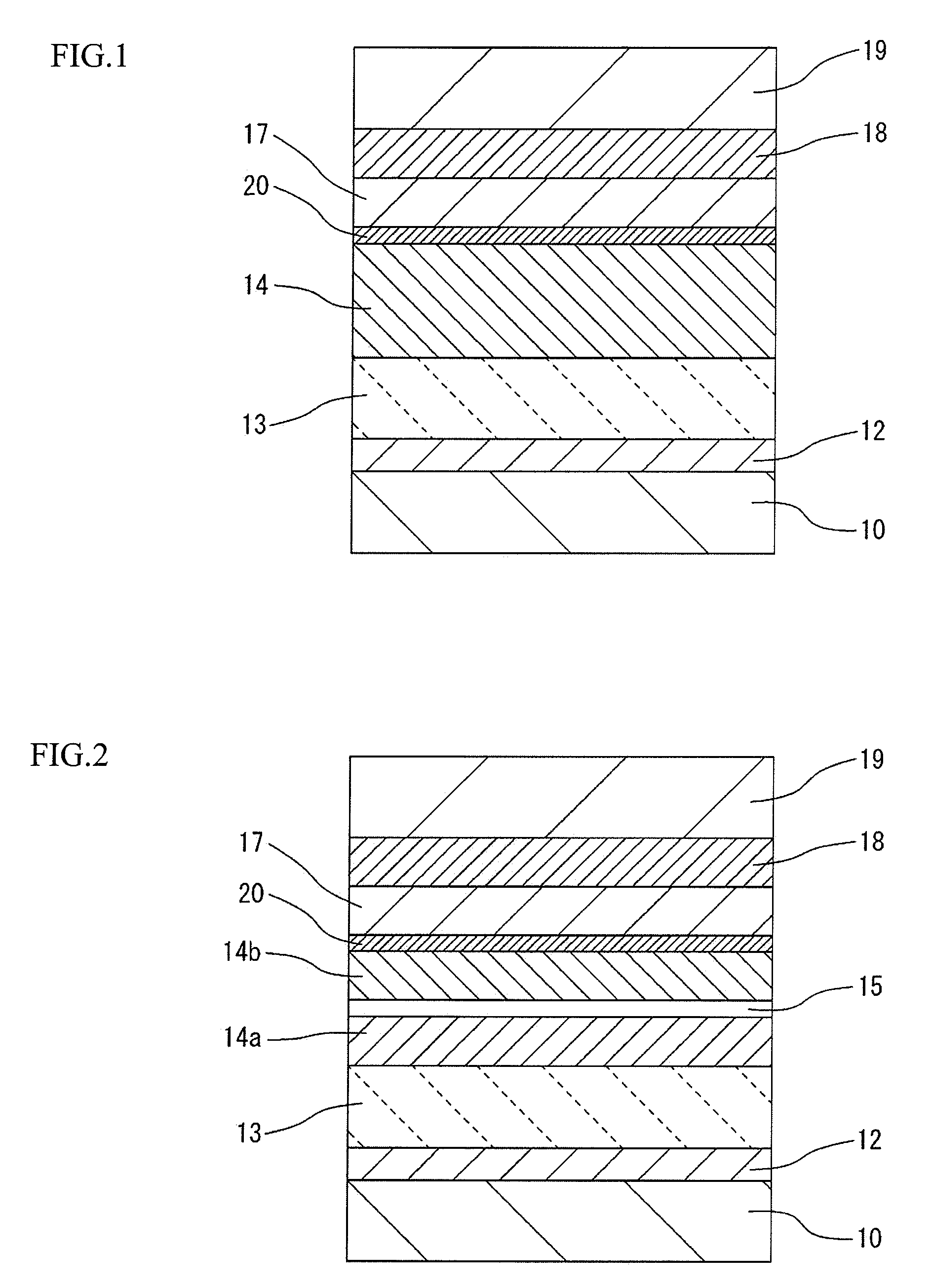
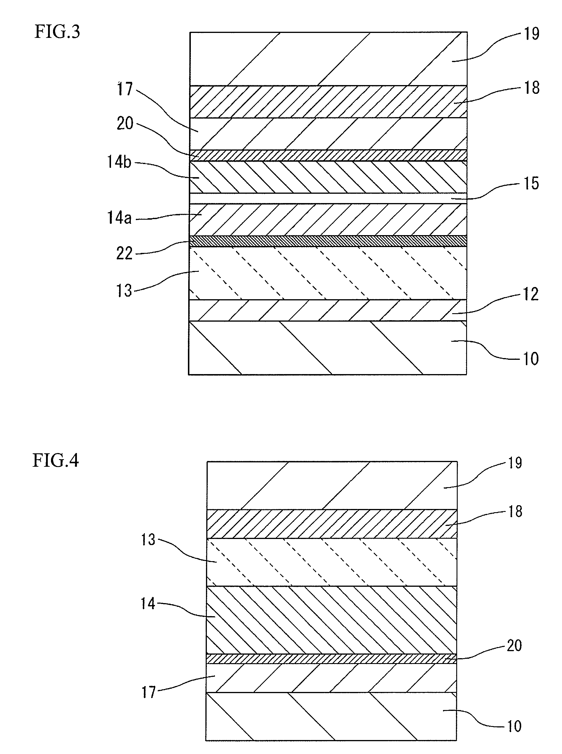
[0042]In the first embodiment, as shown in FIG. 1, a lower shielding layer 10, a base layer 12, an antiferromagnetic layer 13, a pinned magnetic layer 14, a barrier layer 20, a free layer 17, a cap layer 18 and an upper shielding layer 19 are laminated in this order.

[0043]The lower shielding layer 10 is composed of a soft magnetic material, e.g., NiFe, and formed by plating or sputtering. The lower shielding layer 10 serves as an electrode of the TMR element. Note that, in the following description, the layers are formed by sputtering unless otherwise explained. However, the method of forming the layers is not limited to sputtering.

[0044]The base layer 12, which is a two-layered film composed of Ta / Ru, serves as a base of the antiferromagnetic layer 13, which is composed of an antiferromagnetic material including Mn.

[0045]The antiferroma...

second embodiment

[0058]Next, the magnetoresistance effect element of the present invention will be explained. Note that, the structural elements described in the foregoing embodiment are assigned the same symbols.

[0059]In FIG. 2, the pinned magnetic layer 14, which has been explained in the first embodiment, is constituted by a first pinned magnetic layer 14a, a second pinned magnetic layer 14b and an antiferromagnetic coupling layer 15, which couples the pinned magnetic layers 14a and 14b. With this structure, the magnetizing direction of the second pinned magnetic layer 14b can be tightly fixed. Namely, in a magnetoresistance effect element, the resistance variation, which is caused by changing the relative angle between the magnetizing direction of the free layer and that of the pinned magnetic layer, is detected, so that a great effect can be obtained by tightly fixing the magnetizing direction of the pinned magnetic layer.

[0060]For example, the first and second pinned magnetic layers 14a and 14...

third embodiment

[0061]Next, the magnetoresistance effect element of the present invention will be explained. Note that, the structural elements described in the foregoing embodiments are assigned the same symbols.

[0062]As shown in FIG. 3, the basic film structure is similar to that of the second embodiment, but an Mn layer 22 is provided between the antiferromagnetic layer 13 composed of the antiferromagnetic material including Mn and the first pinned magnetic layer 14a. With this structure, the function of fixing the magnetizing direction of the pinned magnetic layer can be improved.


PUM

PropertyMeasurementUnit
thicknessaaaaaaaaaa
thicknessaaaaaaaaaa
thicknessaaaaaaaaaa

Abstract

The high quality magnetoresistance effect element is capable of reducing resistance in the perpendicular-plane direction and preventing performance deterioration of a barrier layer. The magnetoresistance effect element comprises: a free layer; a pinned magnetic layer; and a barrier layer being provided between the free layer and the pinned magnetic layer, and the barrier layer is composed of a semiconductor.

Description

BACKGROUND OF THE INVENTION[0001]The present invention relates to a magnetoresistance effect element and a magnetoresistive device, more precisely relates to a magnetoresistance effect element, whose barrier layer is composed of a semiconductor, and a magnetoresistive device using the magnetoresistance effect element.[0002]A tunneling magnetoresistance (TMR) element is an example of magnetoresistance effect elements having barrier layers.[0003]Tunneling magnetoresistance effect was firstly reported in 1975, and a laminated film including a barrier layer composed of alumina (AlO), which has a great MR ratio, e.g., 10% or more, at room temperature, was reported. Since then, research and development of the laminated film have been accelerated to apply the film to next-generation magnetic heads of hard disk drive units, magnetoresistive random access memories (MRAM), etc.[0004]Further, TMR effect films including barrier layers composed of magnesium oxide (MgO), which had significantly g...

Claims


Application Information

Patent Timeline
Patent Type & Authority Applications(United States)
IPC IPC(8): G11B5/127G11B5/39
CPCB82Y10/00B82Y25/00G01R33/093Y10T428/1121G11B5/3909G11B5/3993G11C11/16G11B5/3906G11C11/161G11B5/39H01L27/105H10N50/10
Inventor UEHARA, YUJIKOMAGAKI, KOUJIROKAWASAKI, MASASHI
Owner FUJITSU LTD
Why Eureka
Try Eureka