Charge trapping memory cell having bandgap engineered tunneling structure with oxynitride isolation layer

a charge-trapping memory cell and tunneling structure technology, applied in the field of flash memory technology, can solve the problems of limiting the ability to increase the density of flash memory, affecting the speed of erase, and affecting the endurance and charge retention characteristics of memory cells relative to traditional floating gate technology, so as to achieve the effect of increasing the speed of erase in the hole tunneling

Active Publication Date: 2012-05-01
MACRONIX INT CO LTD
View PDF9 Cites 5 Cited by
  • Summary
  • Abstract
  • Description
  • Claims
  • Application Information

AI Technical Summary

Benefits of technology

[0009]The performance achieved using BE-SONOS devices characterized by having a dielectric tunneling structure including a tunneling layer, a band offset layer and an isolation layer as described above, is further improved by engineering the isolation layer, replacing the pure silicon oxide layer with a silicon oxynitride (SiOxNy— hereinafter SiON), where the thickness of the isolation layer and the concentration of nitrogen are set so that charge retention is maintained or improved and hole tunneling erase speeds are increased.
[0010]SiON can be fabricated with ranges in values for the dielectric constant K, the band gap, and the conduction band and valence band barrier heights ranging from those of silicon dioxide SiO2 and silicon nitride Si3N4. By reducing the valence band barrier height (increasing nitrogen concentration), the speed of erase by hole tunneling is improved. Meanwhile, the SiON isolation layer can be implemented with sufficient barrier height and thickness to prevent charge loss during operating modes in which charge retention is important.
[0012]The valence band energy level at the first offset is such that an electric field sufficient to induce hole tunneling through the thin region between the interface with the semiconductor body and the offset, is also sufficient to raise the valence band energy level after the offset to a level that effectively eliminates the hole tunneling barrier in the engineered tunneling dielectric after the offset at lower electric field magnitudes than are possible using the prior art BE-SONOS devices. This structure enables electric field assisted hole tunneling at high speeds while effectively preventing charge leakage (improving data retention) through the engineered tunneling dielectric in the absence of electric fields or in the presence of smaller electric fields induced for the purpose of other operations, such as reading data from the cell or programming adjacent cells.

Problems solved by technology

As the density increases in memory devices, and the floating gate memory cells get closer and closer together, interference between the charge stored in adjacent floating gates becomes a problem.
This interference limits the ability to increase the density of flash memory based on floating gate memory cells.
However at that thickness, the endurance and charge retention characteristics of the memory cell are poor relative to traditional floating gate technology.
However, if the erase saturation level is too high, the cell cannot be erased at all, or the threshold margin between the programmed and erased states becomes too small for many applications.
While the BE-SONOS structure provides excellent reliability, the erase speed remains limited.

Method used


Image

  • Charge trapping memory cell having bandgap engineered tunneling structure with oxynitride isolation layer
  • Charge trapping memory cell having bandgap engineered tunneling structure with oxynitride isolation layer
  • Charge trapping memory cell having bandgap engineered tunneling structure with oxynitride isolation layer

Examples


Embodiment Construction

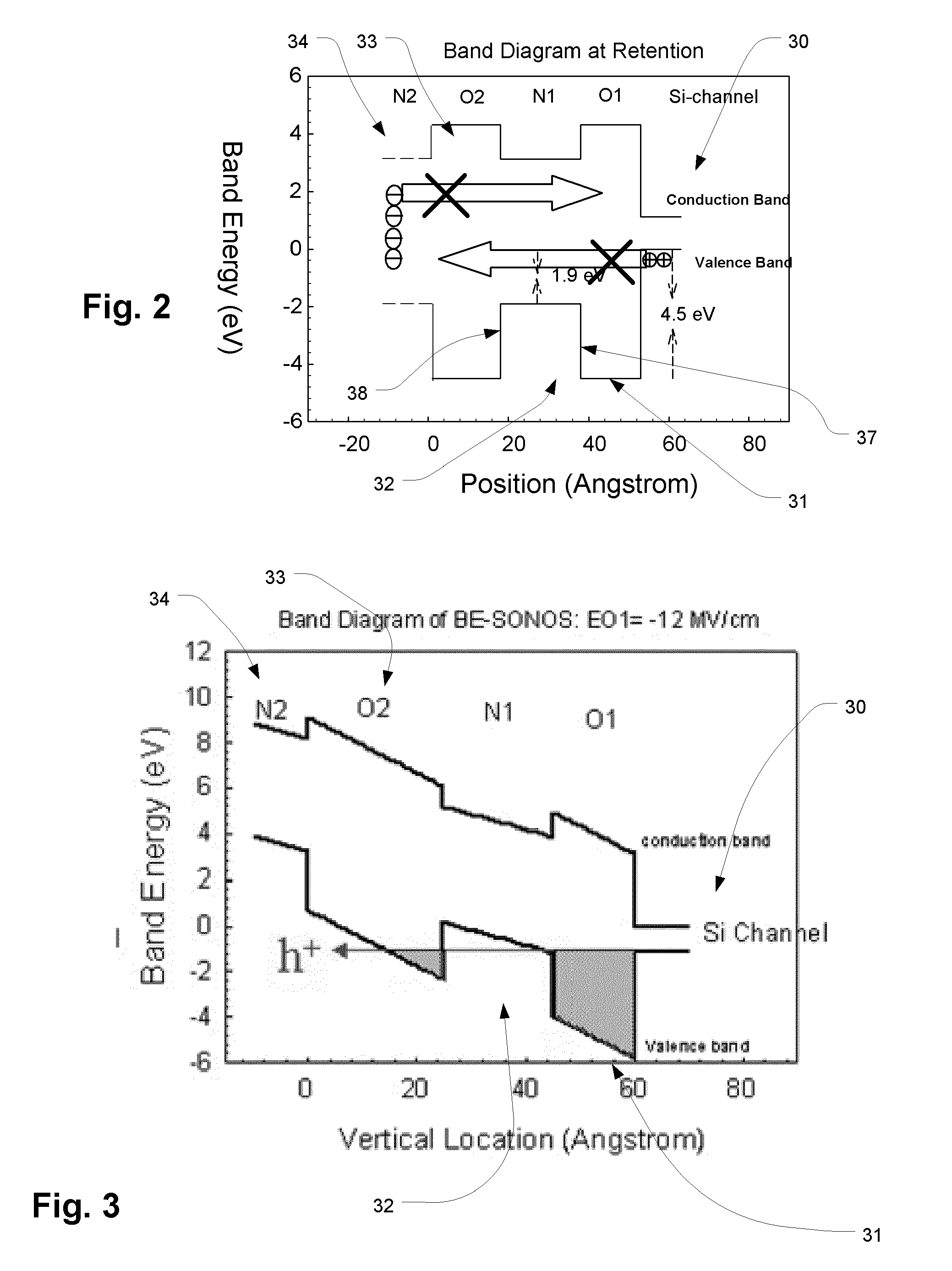
[0042]A detailed description of embodiments of the present invention is provided with reference to the FIGS. 1-24.

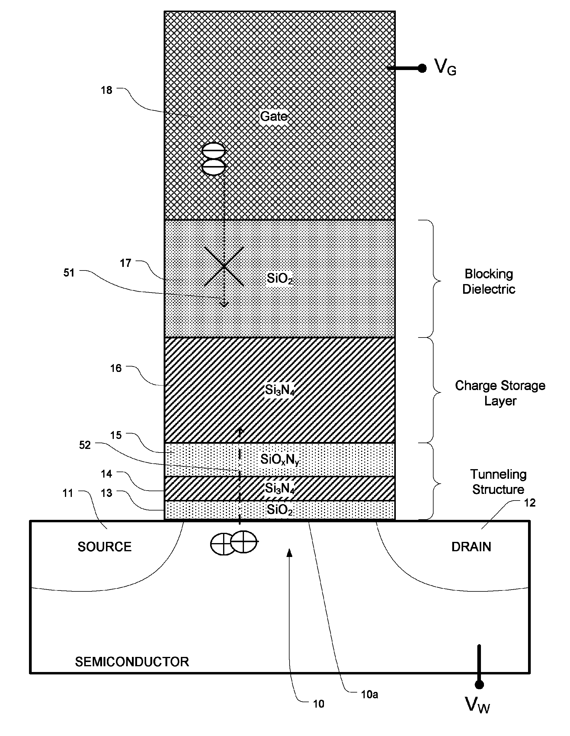
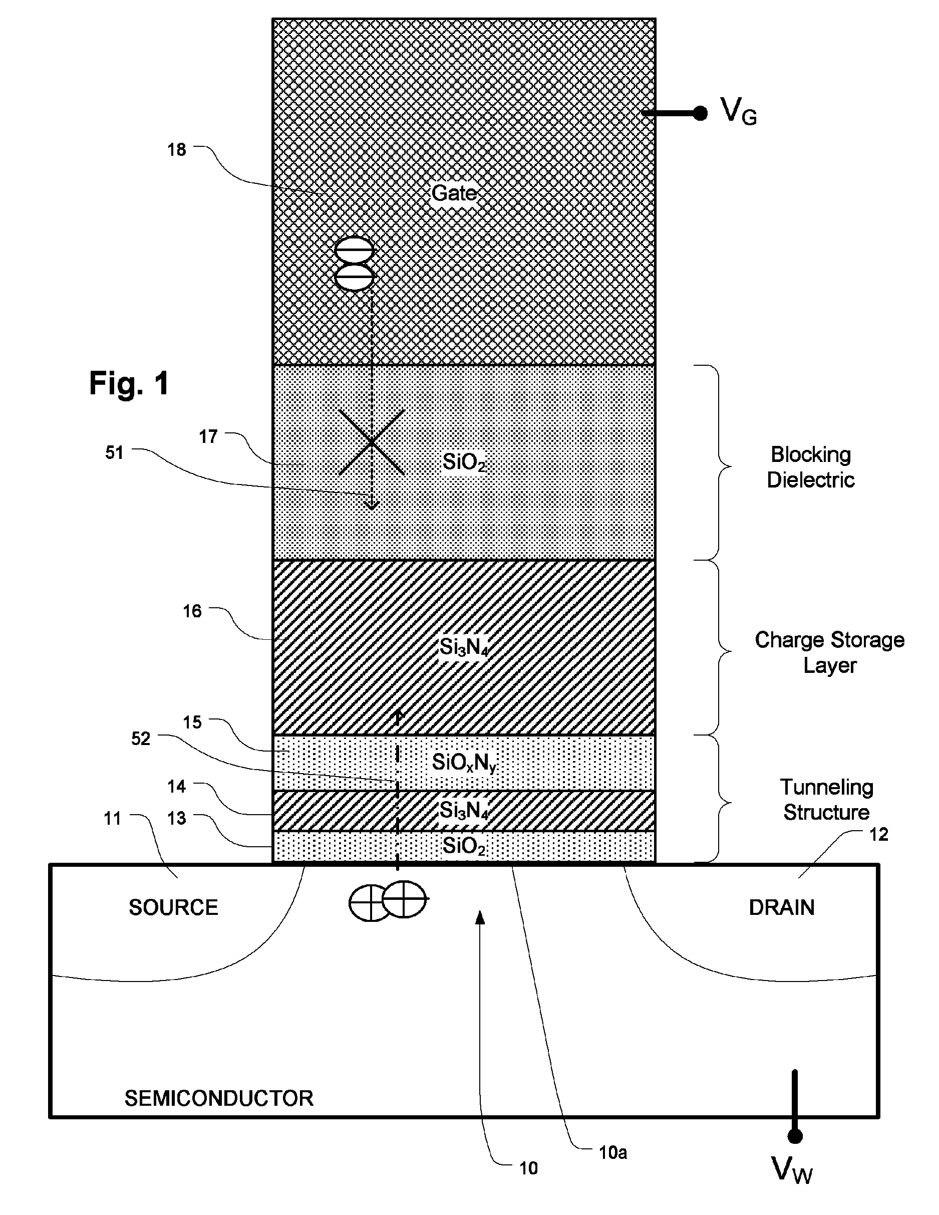
[0043]FIG. 1 is a simplified diagram of a charge trapping memory cell employing a band gap engineered dielectric tunneling layer, including an isolation layer consisting of SiON. The memory cell includes a channel 10 in a semiconductor body, and a source 11 and a drain 12 adjacent channel. FIG. 1 includes schematic symbols for hole tunneling 52 in the dielectric tunneling structure (layers 13-15) and electron tunneling 51 in the blocking layer 17 as induced in an erase process, discussed below.

[0044]A gate 18 in this embodiment comprises p+ polysilicon. N+ polysilicon may also be used. Other embodiments employ metals, metal compounds or combinations of metals and metal compounds for the gate 18, such as platinum, tantalum nitride, metal silicides, aluminum or other metal or metal compound gate materials. For some applications, it is preferable to use materials having wor...


PUM


Abstract

A band gap engineered, charge trapping memory cell includes a charge storage structure including a trapping layer. a blocking layer, and a dielectric tunneling structure including a thin tunneling layer, a thin bandgap offset layer and a thin isolation layer comprising silicon oxynitride. The memory cell is manufactured using low thermal budget processes.

Description

BACKGROUND OF THE INVENTION[0001]1. Field of the Invention[0002]The present invention relates to flash memory technology, and more particularly to scalable charge trapping memory technology adaptable for high speed erase and program operations.[0003]2. Description of Related Art[0004]Flash memory is a class of non-volatile integrated circuit memory technology. Traditional flash memory employs floating gate memory cells. As the density increases in memory devices, and the floating gate memory cells get closer and closer together, interference between the charge stored in adjacent floating gates becomes a problem. This interference limits the ability to increase the density of flash memory based on floating gate memory cells. Another type of memory cell used for flash memory can be referred to as a charge trapping flash memory cell, which uses a dielectric charge trapping layer in place of the floating gate. Charge trapping memory cells use dielectric charge trapping material that cau...

Claims


Application Information

Patent Timeline
Patent Type & Authority Patents(United States)
IPC IPC(8): G11C16/04
CPCH01L21/28282H01L27/11568H01L29/792H01L29/513H01L29/518H01L29/4234H01L29/40117H10B43/30
Inventor LIAO, JENG-HWASHIEH, JUNG-YUYANG, LING-WUU
Owner MACRONIX INT CO LTD
Why Eureka
Try Eureka