Standard cell, standard cell library, semiconductor device, and placing method of the same

Inactive Publication Date: 2006-06-29
SOCIONEXT INC
View PDF1 Cites 24 Cited by
  • Summary
  • Abstract
  • Description
  • Claims
  • Application Information

AI Technical Summary

Benefits of technology

[0044] Also in the present invention, a power source capacitor cell is provided in a region in which a consumed current amount exceeds an arbitrary reference. Thereby, the number of power source capacitor cells to be inserted is limited, so that an increase in area can be suppressed. In addition, when standard cells having different well heights coexist, a semiconductor device in which the area of each standard cell is minimized can be realized.
[0045] As described above, according to the present invention, for example, a space occurring when a small element, such as a low-perform

Problems solved by technology

However, in the case where standard cells have the same high height and the well border lines thereof have the same height, when a transistor having a low level of performance (i.e., a so-called small-size transistor) is realized, a useless region may occur and therefore the area efficiency may be reduced. FIG. 32 is a diagram illustrating a specific example of this situation, i.e., a standard cell which has a CMOS structure employing a small-size transistor and has a low level of area efficiency.
When the low-performance transistors are provided in the standard

Method used


Image

  • Standard cell, standard cell library, semiconductor device, and placing method of the same
  • Standard cell, standard cell library, semiconductor device, and placing method of the same
  • Standard cell, standard cell library, semiconductor device, and placing method of the same

Examples


first example

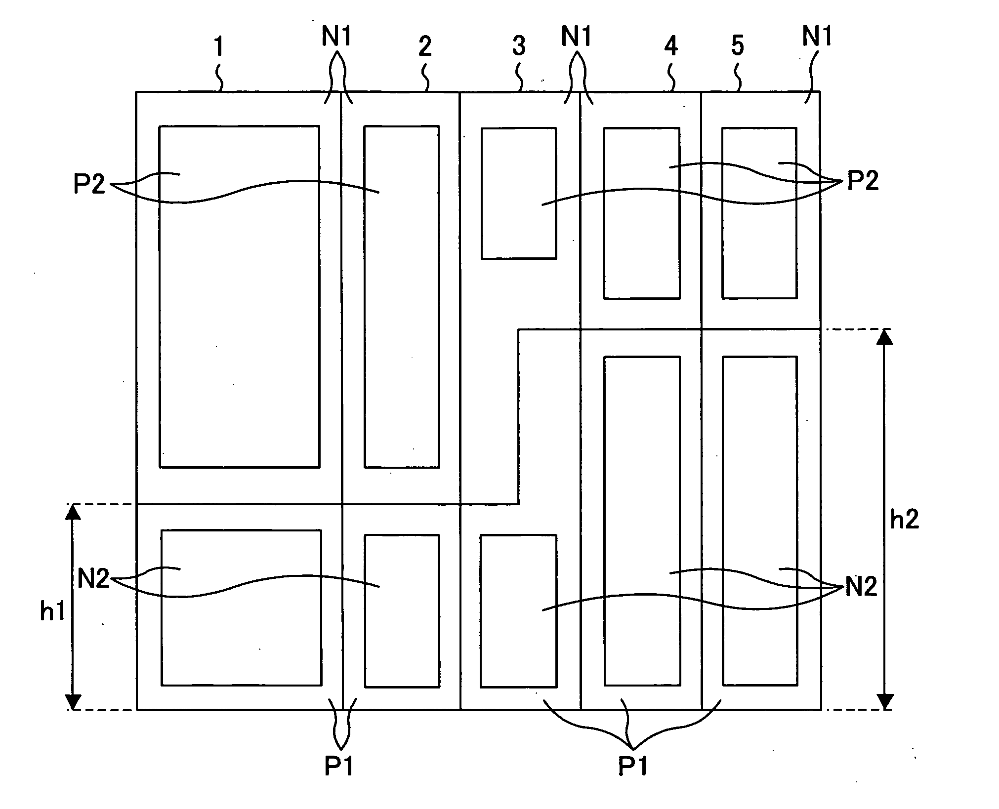
[0080]FIG. 1 is a standard cell placement diagram illustrating an exemplary layout of a standard cell semiconductor device according to a first example of the present invention. Note that standard cells indicated with the same reference numeral are identical to each other throughout the drawings in the first example or later.

[0081] In FIG. 1, 1 to 5 each indicate a standard cell. Each standard cell comprises an N-well region N1 (upper side) and a P-well region P1 (lower side). The N-well region N1 has a P-type diffusion region (P-type active region) P2 for forming a P-channel transistor, and the P-well region P1 has an N-type diffusion region (N-type active region) N2 for forming an N-channel transistor.

[0082] In the standard cells 1 to 5, a large-size transistor is realized by setting the height of the standard cell to be high without dividing into a plurality of standard cells using a parallel structure, thereby preventing a reduction in the area efficiency and a reduction in th...

second example

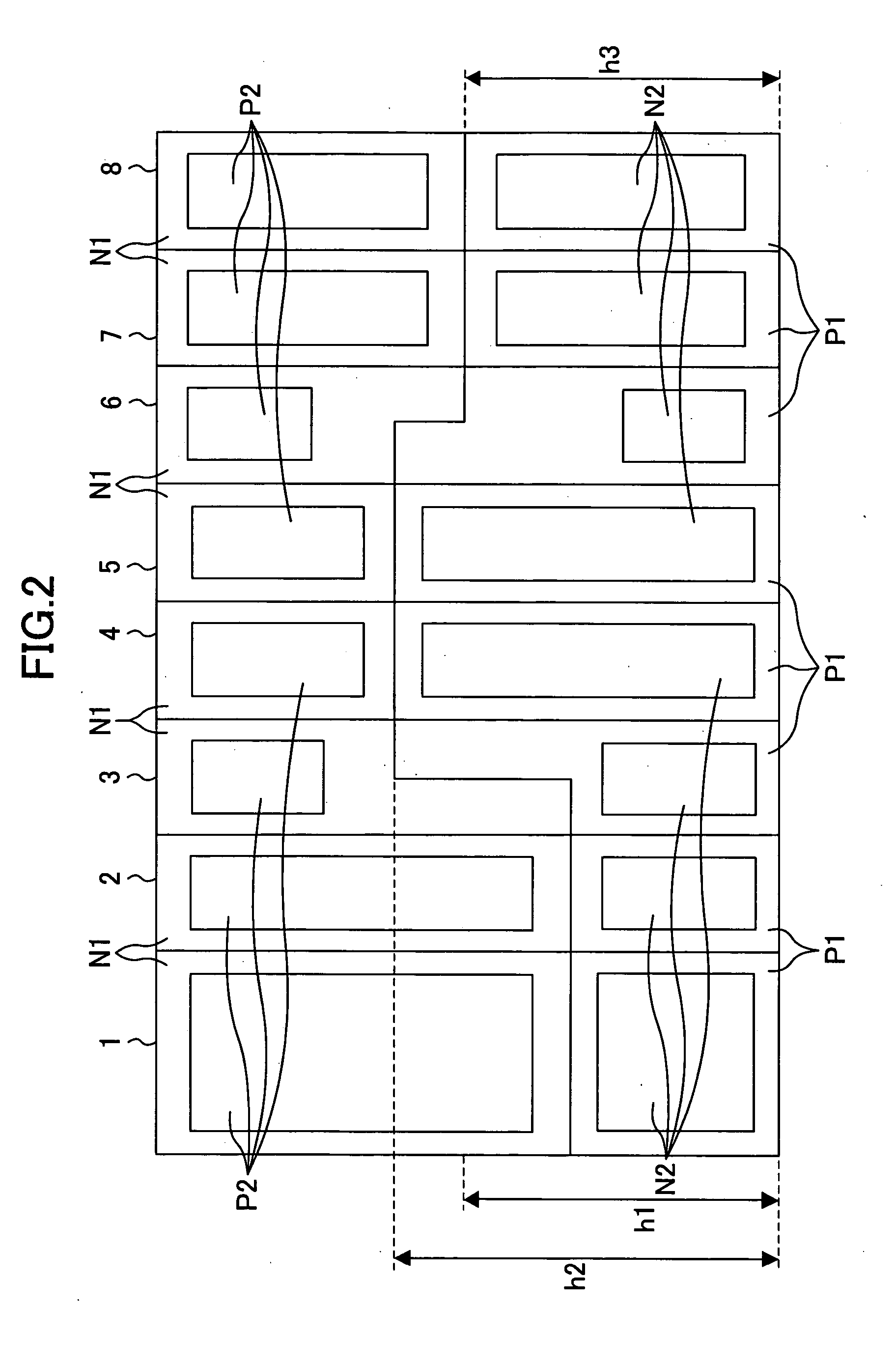
[0087]FIG. 2 is a standard cell placement diagram illustrating an exemplary layout of a standard cell semiconductor device according to a second example of the present invention.

[0088] Standard cells 1 and 2 are first standard cells in which a size of the P-channel transistor is larger than that of the N-channel transistor, a size of the P-type diffusion region P2 is larger than that of the N-type diffusion region N2, and the P-well region P1 has a height h1 (first height) at both ends thereof. Standard cells 4 and 5 are second standard cells in which a size of the N-channel transistor is larger than that of the P-channel transistor, a size of the N-type diffusion region N2 is larger than that of the P-type diffusion region P2, and the P-well region P1 has a height h2 (second height) which is different from h1, at both ends thereof. Standard cells 7 and 8 are fourth standard cells in which a size of the N-channel transistor is equal to that of the P-channel transistor, and the P-we...

third example

[0096]FIG. 3 is a flowchart illustrating a placing method for a semiconductor device according to a third example of the present invention. FIGS. 4 to 8 are diagrams illustrating a result of placement of standard cells based on the placing method of FIG. 3, and the standard cells. Hereinafter, the placing method of FIG. 3 will be described with reference to FIGS. 4 to 8.

[0097] In FIG. 3, S101 is a standard cell placing step of providing an initial placement in which standard cells having different well border line heights coexist.

[0098]FIG. 4 is a standard cell placement diagram illustrating a result of the placement in the standard cell placing step S101. Standard cells 104, 105, 108, 109, and 111 are each a standard cell (first standard cell) whose P-well region has a height h101 (first height). Standard cells 106, 107, and 110 are each a standard cell (second standard cell) whose P-well region has a height h102 (second height) which is different from the height h1.

[0099] At th...


PUM


Abstract

Of a plurality of standard cells in which an N-well region and a P-well region are vertically formed, some standard cells have a border line between the N-well region and the P-well region which is set to be a low height (first height), and other standard cells have a border line between the N-well region and the P-well region which is set to be a high height (second height), depending on the size of a transistor formed in the standard cell. Although these standard cells have different border lines, a standard cell for linking the border lines is provided. In such a standard cell, an empty space is created by forming a small-size transistor therein, and the empty space is utilized so that, for example, a left end of the border line is set to have the first height and a right end of the border line is set to have the second height, whereby the border line is converted so as to link the heights therein.

Description

CROSS REFERENCE TO RELATED APPLICATIONS [0001] This Non-provisional application claims priority under 35 U.S.C. §119(a) on Patent Application No. 2004-366515 filed in Japan on Dec. 17, 2004 and Patent Application No. 2005-331926 filed in Japan on Nov. 16, 2005, the entire contents of which are hereby incorporated by reference.BACKGROUND OF THE INVENTION [0002] 1. Field of the Invention [0003] The present invention relates to a standard cell, a standard cell library, a semiconductor device, and a placing method of the same. [0004] 2. Description of the Related Art [0005] In conventional standard cell semiconductor devices, a number of standard cells are supposed to have substantially the same height so that they can be placed without a gap, i.e., with high density. Further, the cells have the same height of a border line between a P-well region and an N-well region (hereinafter referred to as a well border line height) so that an area efficiency of each individual standard cell is in...

Claims


Application Information

Patent Timeline
IPC IPC(8): H01L27/10
CPCG06F17/5072H01L27/0207H01L27/11807G06F30/392
Inventor SHIMAMURA, AKIMITSU
Owner SOCIONEXT INC
Why Eureka
Try Eureka