
Negative voltage level converting circuit

A technology for converting circuits and negative voltages, applied in the direction of logic circuit connection/interface layout, logic circuit coupling/interface using field effect transistors, static memory, etc., which can solve the problem of increasing the complexity of the manufacturing process and undisclosed negative voltage level conversion The same or similar circuits and other issues, to achieve the effect of low power consumption and fast level conversion speed

Inactive Publication Date: 2005-05-04
TSINGHUA UNIV
View PDF0 Cites 0 Cited by
  • Summary
  • Abstract
  • Description
  • Claims
  • Application Information

AI Technical Summary

Problems solved by technology

Further experiments show that for traditional negative high-voltage level shifting circuits, the normal operation of the circuit can only be guaranteed when the power supply voltage does not decrease, which limits the ability to reduce the size of high-voltage transistors and increases the complexity of the manufacturing process
[0011] After searching, there is no disclosure of the same or similar circuit as the negative voltage level conversion circuit proposed by the present invention in the existing patent literature and non-patent literature

Method used


Image

  • Negative voltage level converting circuit
  • Negative voltage level converting circuit
  • Negative voltage level converting circuit

Examples


Embodiment Construction

[0024] The specific embodiment of the present invention will be described with reference to the accompanying drawings.

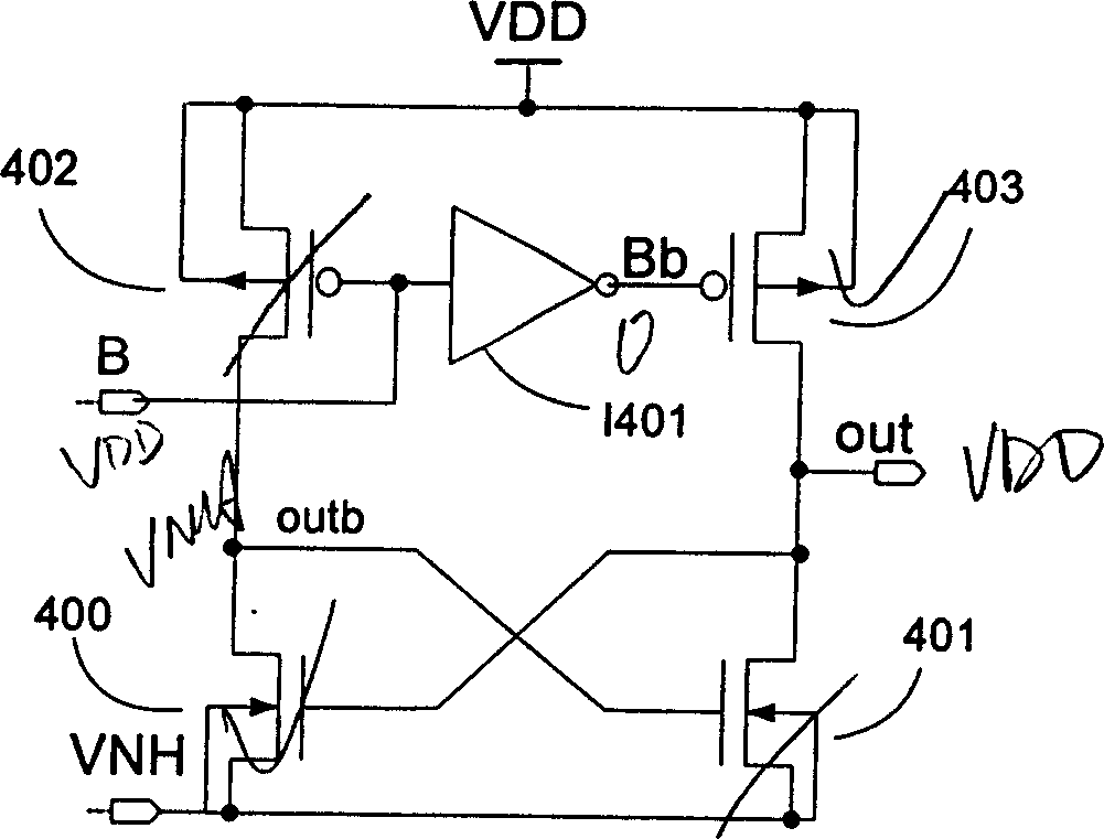
[0025] Figure 4 It is the negative voltage level conversion circuit proposed by the present invention, which is composed of high-voltage PMOS transistors 503-506, high-voltage NMOS transistors 501, 502 and a CMOS inverter 507 working at VDD voltage.

[0026] The drain of the high-voltage PMOS transistor 504 is connected to the node outb (the drain of the NMOS transistor 501 ), the gate is connected to the output node out (the drain of the NMOS transistor 502 ), and the source is connected to the input terminal A. The drain of the high-voltage PMOS transistor 505 is connected to the node outb, the gate is fixedly grounded, and the source is connected to the input terminal A. The drain of the high-voltage PMOS transistor 503 is connected to the output node out, the gate is connected to the node outb, and the source is connected to the output terminal B of th...


PUM


Abstract

The negative voltage level conversion circuit belongs to the technical field of mixed signal processing integrated circuit and non-volatile memory circuit design. It is characterized in that it contains: two inverters composed of PMOS transistors and NMOS transistors respectively, the input and output ends of the two inverters are connected to each other to form a positive feedback channel of the output voltage, and the output positive high voltage is inverted by one of them. The negative voltage is transmitted by the PMOS tube of the phase device, and the negative low voltage is transmitted by the NMOS tube. This positive feedback channel speeds up the speed of level conversion; a CMOS inverter working under the input voltage makes the branch currents on both sides asymmetrical, and reduces The power consumption required for conversion is reduced; the initial input voltage of the two inverters is determined by two PMOS transistors whose gates are grounded. The invention has fast level conversion speed, can still work normally when the input voltage is lowered, and increases the ability of reducing the size of the transistor.

Description

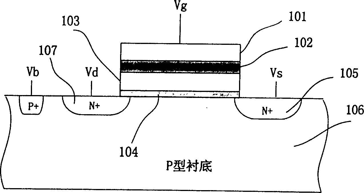
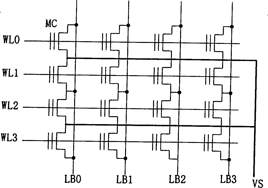
technical field [0001] The negative voltage level conversion circuit relates to the technical fields of mixed signal processing integrated circuit and non-volatile memory circuit design. Background technique [0002] Currently, among non-volatile memories, flash memory (Flash Memory) is developing rapidly due to its high programming speed, high integration and superior performance. In 1984, Masuoka and others proposed the concept of flash memory for the first time, that is, the high speed of flash erasing was realized by erasing and programming by bit and bit by block (sector), and eliminated EEPROM (Erasable Programmable Read-only memory: Erasable Programmable Read-only memory: Erasable Programmable Read-only memory) necessary selector for programming read-only memory). [0003] figure 1 is a cross-sectional view of a traditional flash memory unit, which is a stacked gate structure composed of a polysilicon floating gate 103 (Floating Gate) and a control gate 101 (Control...

Claims


Application Information

Patent Timeline
Patent Type & Authority Patents(China)
IPC IPC(8): G11C16/06H03K19/0185
Inventor 段志刚潘立阳伍冬朱钧
Owner TSINGHUA UNIV
Learn More