Negative voltage decoding circuit

A decoding circuit, negative voltage technology, applied in logic circuit connection/interface layout, logic circuit coupling/interface using field effect transistors, static memory, etc., can solve problems such as power asymmetry, reduction, and circuit failure , to achieve the effects of small conversion power consumption, reduced maximum voltage, and increased size

Inactive Publication Date: 2004-05-05
TSINGHUA UNIV
View PDF0 Cites 8 Cited by
  • Summary
  • Abstract
  • Description
  • Claims
  • Application Information

AI Technical Summary

Problems solved by technology

A CMOS inverter is also used to make the power supply of the two branches asymmetric, so that the driving current required by the negative high-voltage level shifting circuit during conversion is greatly reduced, thereby overcoming the traditional negative high-voltage level shifting circuit due to the input voltage Defects caused by the circuit not working properly due to lower

Method used


Image

  • Negative voltage decoding circuit
  • Negative voltage decoding circuit
  • Negative voltage decoding circuit

Examples


Embodiment Construction

[0034] The specific embodiment of the present invention will be described with reference to the accompanying drawings.

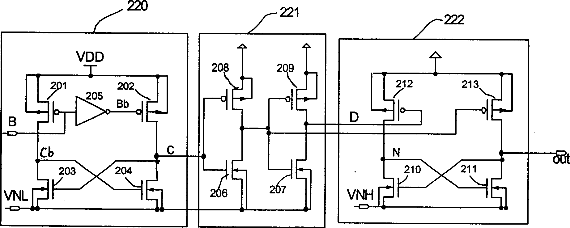
[0035] Figure 4 It is the negative voltage decoding circuit proposed by the present invention, wherein the first-stage negative voltage level conversion circuit is composed of high-voltage PMOS transistors 403-406, high-voltage NMOS transistors 401, 402 and a CMOS inverter 407 working at VDD voltage.

[0036]The drain of the high-voltage PMOS transistor 404 is connected to the node E (the drain of the NMOS transistor 401 ), the gate is connected to the output node C (the drain of the NMOS transistor), and the source is connected to the input terminal A. The drain of the high-voltage PMOS transistor 405 is connected to the node E, the gate is fixedly grounded, and the source is connected to the input terminal A. The drain of the high voltage PMOS transistor 403 is connected to the output node C, the gate is connected to the node E, and the source is connect...


PUM


Abstract

Negative voltage decoding circuit belongs to technique area for designing hybrid signal processing IC and not volatile memory circuit. The characters are as follows. First stage of negative voltage level transfer circuit contains an inverter composed of PMOS tube and NMOS tube as well as a CMOS inverter. The input end and output end of said PMOS tube and NMOS tube are connected so as to constitute positive feedback channel of output voltage. PMOS tube transfers positive voltage, and NMOS tube transfers negative low voltage. CMOS inverter makes asymmetric branch currents at two sides. Two PMOS tubes determine initial input voltage of the two inverters. NMOS tube with its grid electrode being connected to positive high voltage transfers output earth level when the fetch-discharge channel reads level normally. Thus, transferring loss of PMOS tube is avoided. The invention possesses features of fast level conversion speed, increasing capability of reducing size of transistor.

Description

technical field [0001] The negative voltage decoding circuit relates to the technical fields of mixed signal processing integrated circuit and non-volatile memory circuit design. Background technique [0002] Currently, among non-volatile memories, flash memory (Flash Memory) is developing rapidly due to its high programming speed, high integration and superior performance. In 1984, Masuoka and others proposed the concept of flash memory for the first time, that is, the high speed of flash erasing was realized by erasing and programming by bit and bit by block (sector), and eliminated EEPROM (Erasable Programmable Read-only memory: Erasable Programmable Read-only memory: Erasable Programmable Read-only memory) necessary selector for programming read-only memory). [0003] figure 1 Represents the layout of a memory array. When the memory performs an erasing operation on a selected block, it is necessary to add a corresponding erasing voltage (generally a negative voltage) ...

Claims


Application Information

Patent Timeline
Patent Type & Authority Applications(China)
IPC IPC(8): G11C16/16H03K19/0185
Inventor 段志刚潘立阳伍冬朱钧
Owner TSINGHUA UNIV
Why Eureka
Try Eureka