Gate controlling circuit for raising transistor with nigh voltage input
A gate control and transistor technology, applied in logic circuits, electrical components, electronic switches, etc., can solve the problems of input signal can not be turned off by PMOS transistor, TDDB reliability problem, system failure and so on
- Summary
- Abstract
- Description
- Claims
- Application Information
AI Technical Summary
Problems solved by technology
Method used
Image

Examples
Embodiment Construction
[0039] Preferred embodiments according to the present invention will now be described hereinafter with reference to the accompanying drawings.
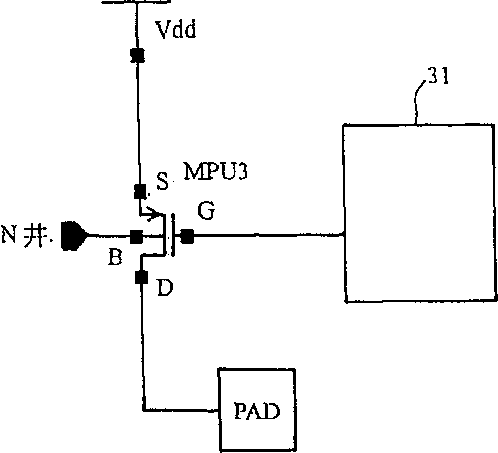
[0040] image 3 shows a schematic circuit diagram including a gate control circuit for a pull-up transistor according to the present invention, in this circuit, the gate terminal G of the pull-up transistor MPU 3 is connected to the gate control circuit 31, the source of the transistor MPU 3 The terminal S is connected to the power supply potential Vdd, the drain terminal D of the transistor MPU 3 is connected to the pad PAD node, and the base B of the transistor MPU 3 is connected to an N-well. image 3 The operation of the circuit is that when a high voltage signal is applied, the gate control circuit 31 is used to control the gate bias voltage of the pull-up transistor MPU 3, that is, the pull-up transistor is controlled by the gate control circuit 31 The gate voltage of the MPU 3, and the well bias of the transistor MPU 3 are con...
PUM
 Abstract
Description
Claims
Application Information
 - R&D
- Intellectual Property
- Life Sciences
- Materials
- Tech Scout
- Unparalleled Data Quality
- Higher Quality Content
- 60% Fewer Hallucinations
Browse by: Latest US Patents, China's latest patents, Technical Efficacy Thesaurus, Application Domain, Technology Topic, Popular Technical Reports.
© 2025 PatSnap. All rights reserved.Legal|Privacy policy|Modern Slavery Act Transparency Statement|Sitemap|About US| Contact US: help@patsnap.com