Built-in-chip vacuum fluorescent display

A display and vacuum technology, applied in the field of built-in chip vacuum fluorescent display, can solve problems such as difficult to design VFD, limited driver chips, etc.

Inactive Publication Date: 2003-03-26
SAMSUNG SDI CO LTD
View PDF1 Cites 5 Cited by
  • Summary
  • Abstract
  • Description
  • Claims
  • Application Information

AI Technical Summary

Problems solved by technology

Therefore, it is difficult to design the structure of the VFD in an appropriate manner since the area where the driver chip is mounted is very limited

Method used


Image

  • Built-in-chip vacuum fluorescent display
  • Built-in-chip vacuum fluorescent display
  • Built-in-chip vacuum fluorescent display

Examples


Embodiment Construction

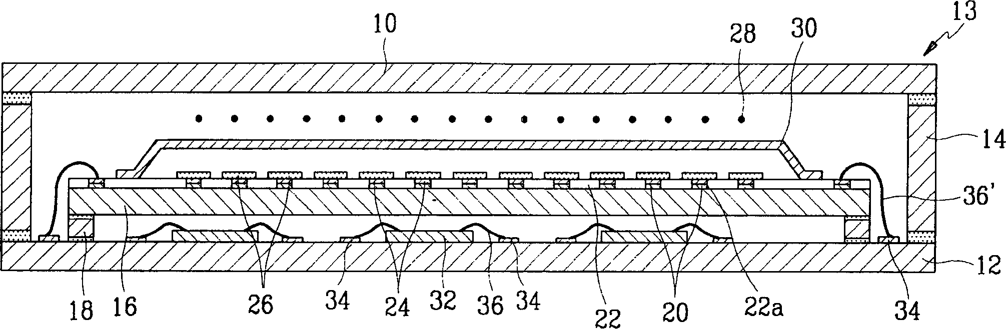
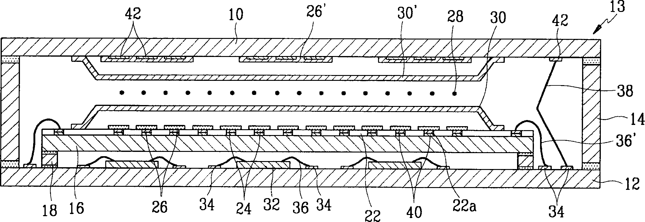
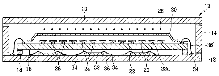
[0018] figure 1 is a cross-sectional view of a built-in chip vacuum fluorescent display according to a first embodiment of the present invention.

[0019] Such as figure 1 As shown, the built-in chip vacuum fluorescent display includes a transparent upper substrate 10, a lower substrate 12 facing the upper substrate 10 and spaced apart from each other, and a side glass 14 disposed between the substrates 10 and 12 and interconnecting them, thereby forming a vacuum tube 13.

[0020] The upper and lower substrates 10 and 12 become main substrates for forming the vacuum tube 13 . In the vacuum tube 13 , at least one auxiliary substrate 16 is disposed above the lower substrate 12 , which has a smaller size than the upper and lower substrates 10 and 12 and is supported by a thin glass-based spacer 18 . The auxiliary substrate 16 is separated from the lower substrate 12 by a distance of 1-3 mm.

[0021] A predetermined pattern of the anode wires 20 is formed on the auxiliary subs...


PUM


Abstract

A built-in chip vacuum fluorescent display including a vacuum tube having a transparent top substrate, a bottom substrate facing the top substrate with driver chip wirings while being spaced apart from the top substrate with a predetermined distance, and a side glass disposed between the top and the bottom substrates while interconnecting the top and the bottom substrates. A plurality of driver chips is mounted at the bottom substrate within the vacuum tube while being electrically connected to the driver chip wirings. At least one subsidiary substrate is provided at the space between the top and the bottom substrates within the vacuum tube while having wirings electrically connected to the driver chip wirings. Cathodes are provided between the subsidiary substrate and the top substrate within the vacuum tube to emit thermal electrons. Phosphors are patterned at the subsidiary substrate while being electrically connected to the wirings.

Description

technical field [0001] The invention relates to a vacuum fluorescent display, and more particularly to a built-in chip vacuum fluorescent display, which installs a driving chip inside a vacuum tube. Background technique [0002] In general, vacuum fluorescent displays (VFDs) can be classified into various forms according to structures, display areas, display contents, and driving methods. In particular, VFDs may be classified into a conventional type, a front emission type, and a dual layer type according to a display area. Considering the display content, VFD can be divided into digital display type, character display type and graphic display type. [0003] A graphic display type VFD has a phosphor patterned into a dot matrix corresponding to image signal information and a driver chip for selectively driving grid electrodes. For example, assume that a graphic display type VFD having a 128×128 dot matrix is ​​driven in a quadruple or an eightfold m...

Claims


Application Information

Patent Timeline
Patent Type & Authority Applications(China)
IPC IPC(8): H01J31/15H01J31/12
CPCH01J31/126H01J31/15
Inventor 河盛皓
Owner SAMSUNG SDI CO LTD
Why Eureka
Try Eureka