Edge enhancement method and device for digital image amplifier circuit

A technology for amplifying circuits and digital images, applied in image communication, electrical components, etc., can solve problems such as blurred outlines and memory resource consumption

Inactive Publication Date: 2003-06-04
SUNPLUS TECH CO LTD
View PDF0 Cites 10 Cited by
  • Summary
  • Abstract
  • Description
  • Claims
  • Application Information

AI Technical Summary

Problems solved by technology

[0003] Although the above-mentioned interpolation method can increase the resolution of the image, however, it will also make the profile of the image blurred, so subsequent sharpening processing is necessary to improve the blurred image profile. Subsequent sharpening processing also requires additional memory registers, which will result in consumption of memory resources

Method used


Image

  • Edge enhancement method and device for digital image amplifier circuit
  • Edge enhancement method and device for digital image amplifier circuit
  • Edge enhancement method and device for digital image amplifier circuit

Examples


Embodiment Construction

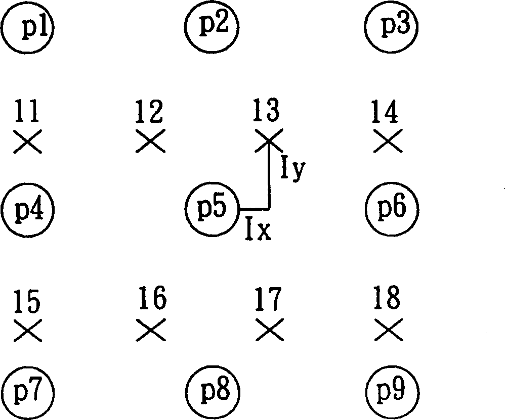
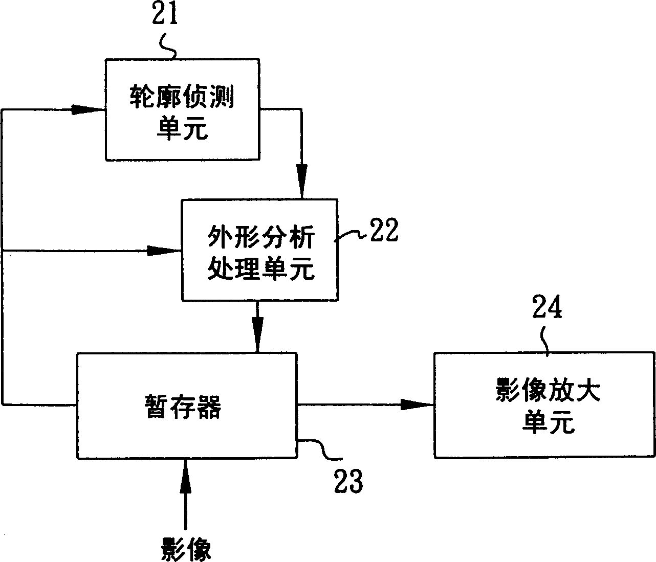
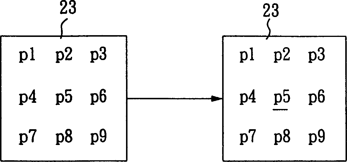
[0025] For a preferred embodiment of the sharpening enhancement method and device of the digital image amplifying circuit of the present invention, please refer to figure 2 As shown, before the image is enlarged (Image Scalar-up), the pixels of the input image are sharpened and flattened by the profile detection unit 21 (Profile Detection) and the outline analysis processing unit 22 (Outline Analytic Process). deal with image 3 As shown, the pixels of the input image to be processed are first stored in the temporary register 23, for example, the originally temporarily stored pixels are P1-P9, and after the pre-processing of sharpening and flattening, the brightness information of the original pixel P5 is replaced by P5, and then the image pixels enter the image enlargement unit 24 to increase the resolution.

[0026] Figure 4 The structure of the aforementioned shape analysis processing unit 22 is shown, which has a high-pass filter 41 and a low-pass filter 42 to filter t...


PUM


Abstract

The present invention is sharpening enhancement method and device for digital image amplifier circuit. Before the amplification of digital image, the contour is detected and the outline is sharpened selectively, and this will reduce the fuzziness degree of the contour without strengthening the noise. After the resolution of the digital image is amplified, the image definition is still maintained. During the outline enhancement treatment, the same temporary memory as that for image amplification is used and this can reduce cost greatly.

Description

technical field [0001] The invention relates to the technical field of digital image amplifying circuits, in particular to a method and device for sharpening digital image amplifying circuits. Background technique [0002] Press, the basic method of general digital image enlargement is to refer to the brightness information of adjacent pixels (Pixel) and use such as nearest neighbor (Nearest Neighbor), bilinear (Bilinear), square (Quadratic), bicubic (Bicubic) or look-up table ( Look Up Table) interpolation (Interpolation) to generate new pixels, such as figure 1 In the part of the image shown, P1-P9 are existing pixels, and I1-I8 are new pixels to be produced, wherein, the positions of I2 and I3 are within the pixel interval of P5, as shown by the dotted line, the two new pixels The luminance information is calculated by combining the luminance information contained in the original pixels P1-P9 with the distance (Ix, Iy) relative to P5. In the calculation process, the coef...

Claims


Application Information

Patent Timeline
Patent Type & Authority Applications(China)
IPC IPC(8): H04N1/40H04N1/409
Inventor 林焜尉陈昶燊
Owner SUNPLUS TECH CO LTD
Why Eureka
Try Eureka