Semiconductor memory device and electronic information apparatus using same

A technology of memory devices and semiconductors, which is applied in the directions of digital memory information, static memory, read-only memory, etc., and can solve the problem of not improving the data readout rate.

Inactive Publication Date: 2003-08-13
SHARP KK
View PDF1 Cites 0 Cited by
  • Summary
  • Abstract
  • Description
  • Claims
  • Application Information

AI Technical Summary

Problems solved by technology

Image 6 The structure shown doe...

Method used


Image

  • Semiconductor memory device and electronic information apparatus using same
  • Semiconductor memory device and electronic information apparatus using same
  • Semiconductor memory device and electronic information apparatus using same

Examples


Embodiment Construction

[0077] Embodiments of the present invention will be described below with reference to the accompanying drawings.

[0078] Referring to FIGS. 1 to 3, a semiconductor memory device 10 according to an example of the present invention will be described. The same units as those shown in FIGS. 4 to 6 are denoted by the same reference numerals, and a detailed description thereof will be omitted.

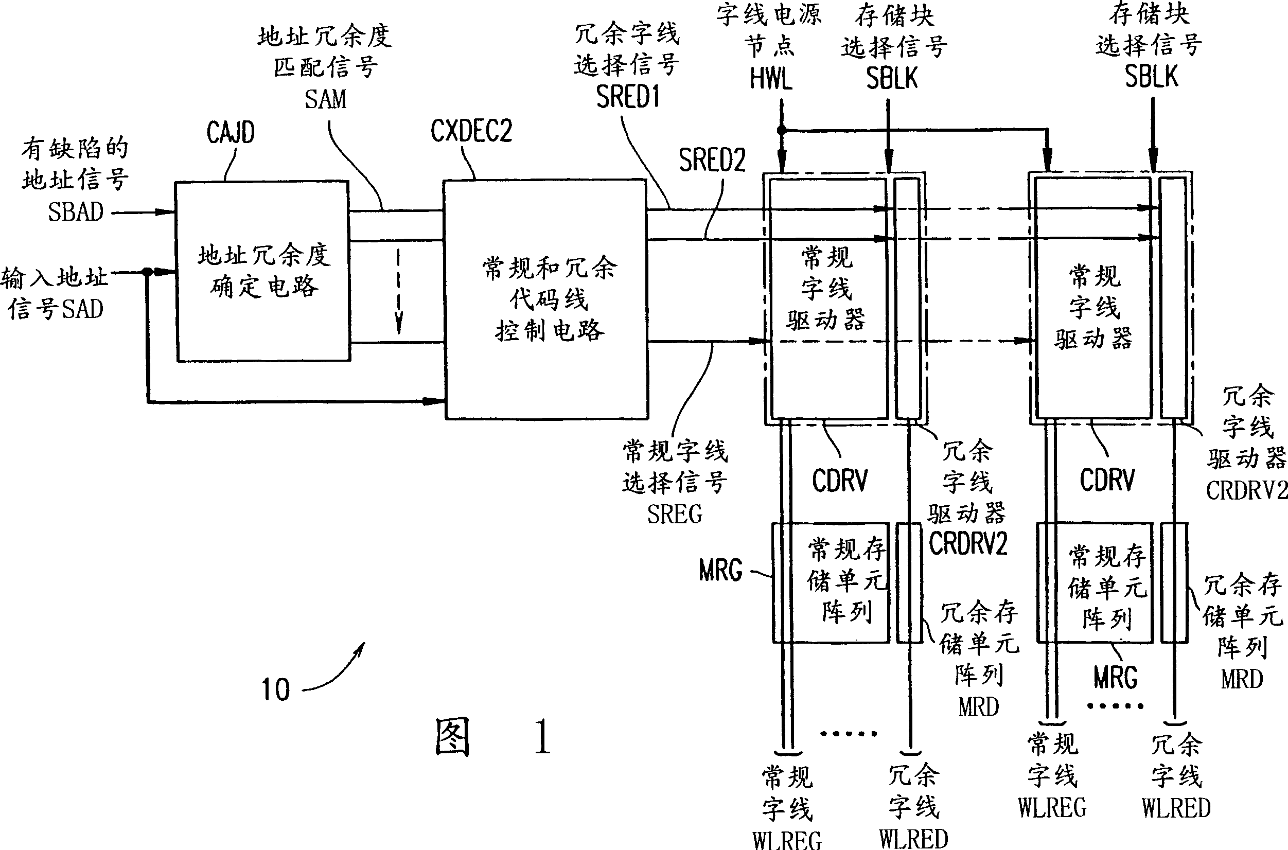
[0079] FIG. 1 is a block diagram illustrating a part of the structure of the semiconductor memory device 10. As shown in FIG.

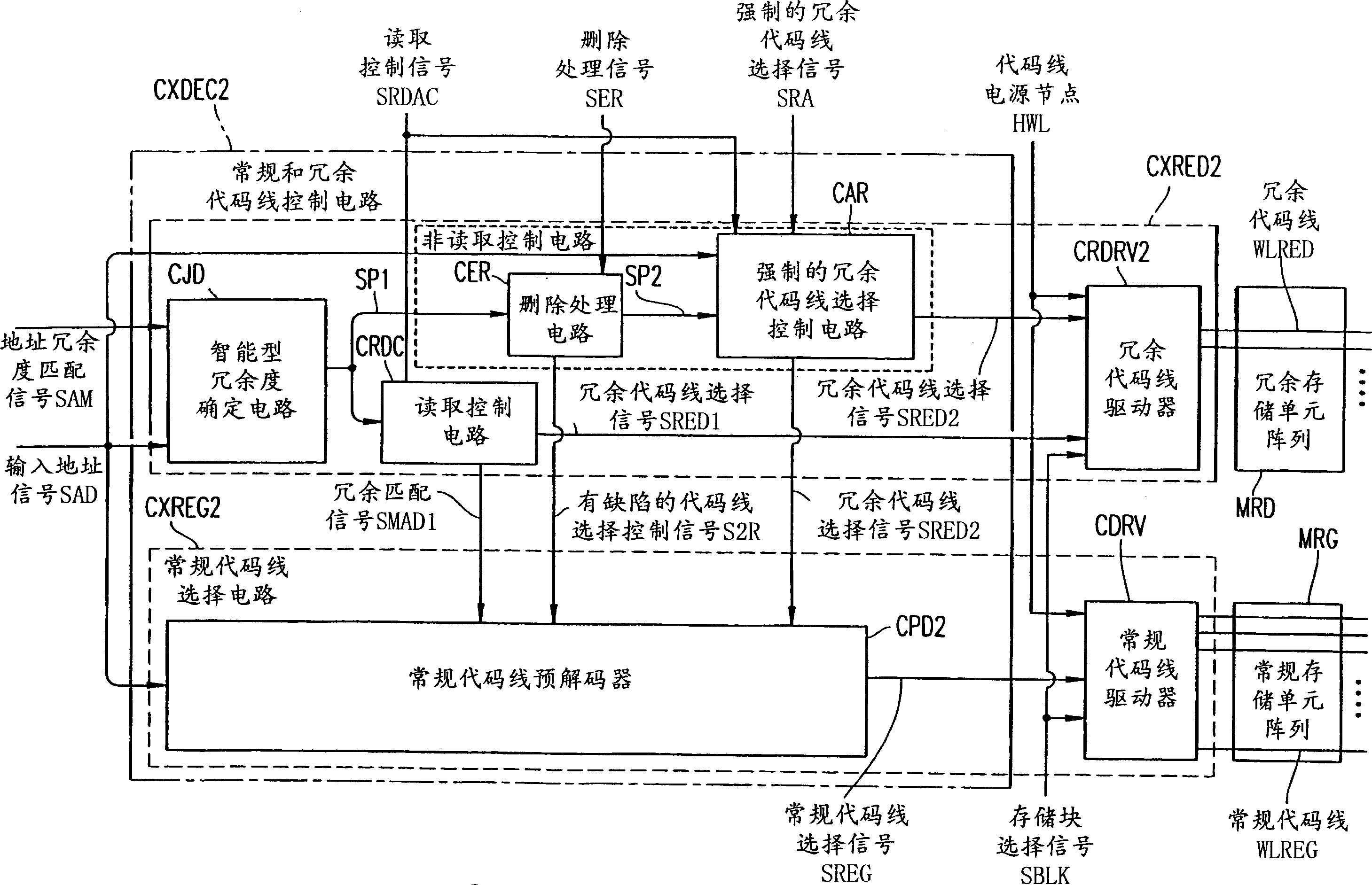
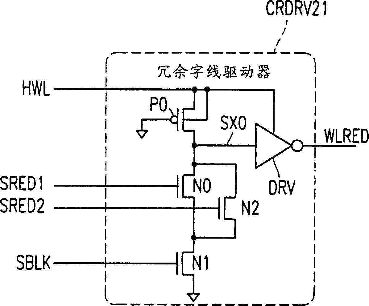
[0080] As shown in FIG. 1, the semiconductor memory device 10 includes an address redundancy determination circuit CAJD, a conventional and redundant word line control circuit CXDEC2, a plurality of conventional memory cell arrays MRG, a plurality of redundant memory cell arrays MRD, a plurality of A normal word line driver CDRV, and a plurality of redundant word line drivers CRDRV2.

[0081] The address redundancy determination circuit CAJD determines whether th...


PUM


Abstract

In a semiconductor memory device, a redundant memory cell is accessible based on an input address signal by a redundant word line selection signal which is output in accordance with whether data read is to be performed or a memory operation other than data read is to be performed.

Description

technical field [0001] The present invention relates to a semiconductor memory device used in electronic information equipment such as a mobile phone, and more particularly, the present invention relates to a nonvolatile semiconductor memory device such as a flash EEPROM. The invention also relates to an electronic information device using the semiconductor storage device. Background technique [0002] In a conventional semiconductor memory device, a non-redundant normal memory cell is accessed based on an input address signal, and when a normal word line for accessing the normal memory cell is defective, a redundant word line to replace the regular word line to access redundant memory cells. [0003] Referring to FIGS. 4 to 6, such a conventional semiconductor memory device will be described. [0004] FIG. 4 is a block diagram illustrating a partial structure of a conventional semiconductor memory device 100. As shown in FIG. More specifically, FIG. 4 shows a partial str...

Claims


Application Information

Patent Timeline
IPC IPC(8): G11C16/06G11C29/00G11C29/04
CPCG11C29/84G11C29/842G11C16/00
Inventor 山野要
Owner SHARP KK
Why Eureka
Try Eureka