Method for accessing semiconductor memory device and electronic information apparatus using same

A storage device and semiconductor technology, applied in the direction of digital memory information, static memory, read-only memory, etc., can solve the problem of not improving the rate of data readout

Inactive Publication Date: 2009-11-18
SHARP KK
View PDF4 Cites 0 Cited by
  • Summary
  • Abstract
  • Description
  • Claims
  • Application Information

AI Technical Summary

Problems solved by technology

Image 6 The structure shown does not improve the rate of data readout

Method used


Image

  • Method for accessing semiconductor memory device and electronic information apparatus using same
  • Method for accessing semiconductor memory device and electronic information apparatus using same
  • Method for accessing semiconductor memory device and electronic information apparatus using same

Examples


Embodiment Construction

[0077] Embodiments of the present invention will be described below with reference to the accompanying drawings.

[0078] refer to figure 1 3 to 3, the semiconductor memory device 10 according to an example of the present invention will be described. and Figures 4 to 6 The same units shown in are denoted by the same reference numerals, and their detailed descriptions will be omitted.

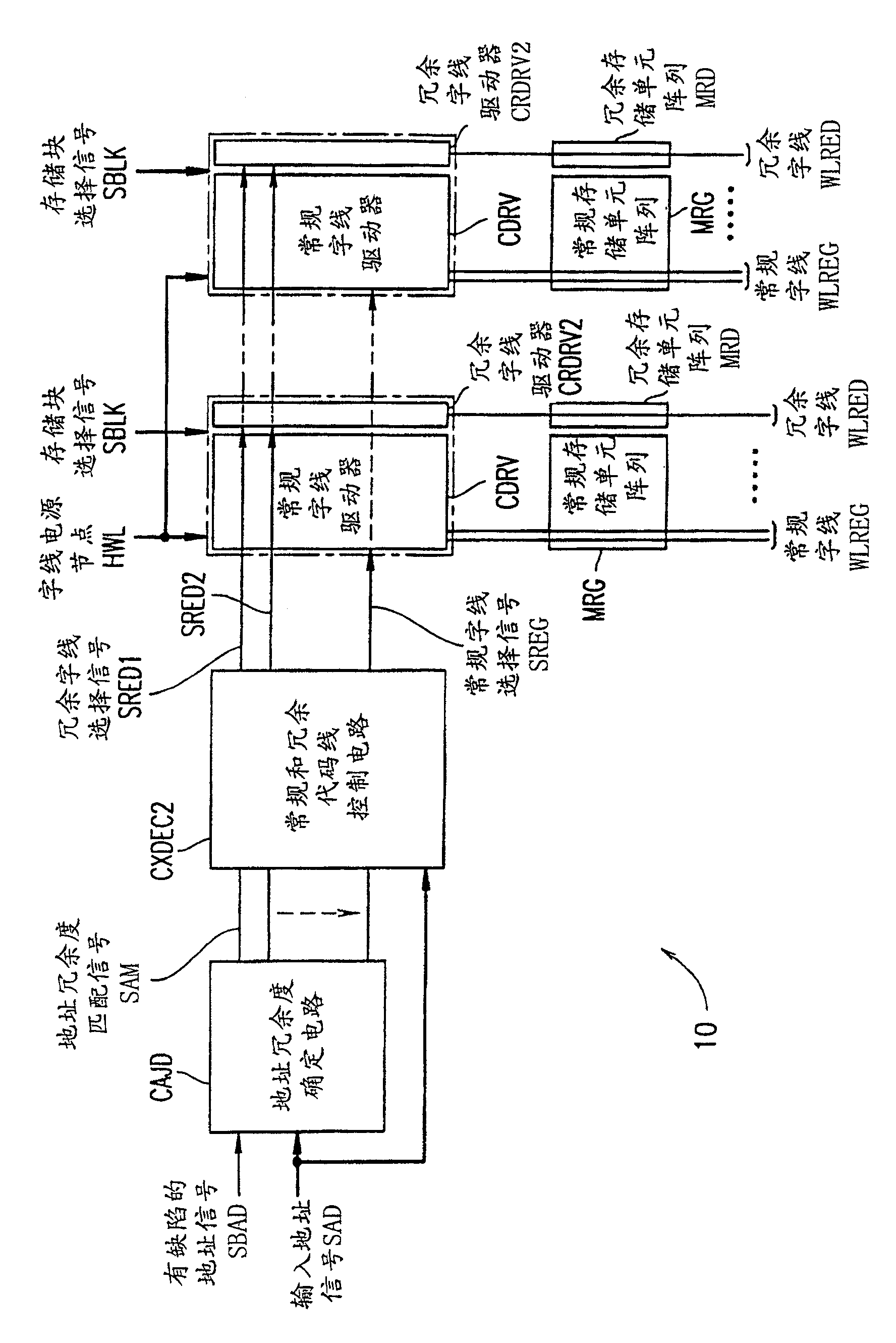
[0079] figure 1 is a block diagram illustrating a part of the structure of the semiconductor memory device 10 .

[0080] Such as figure 1 As shown, the semiconductor memory device 10 includes an address redundancy determination circuit CAJD, a conventional and redundant word line control circuit CXDEC2, a plurality of conventional memory cell arrays MRG, a plurality of redundant memory cell arrays MRD, a plurality of conventional word line line driver CDRV, and a plurality of redundant word line drivers CRDRV2.

[0081] The address redundancy determination circuit CAJD determines whethe...


PUM


Abstract

A semiconductor memory device, wherein, based on an input address signal, redundant memory cells can be accessed by a redundant word line selection signal, the redundant word line selection signal is different according to whether data reading is to be performed or not. It is output during the memory operation of data read.

Description

technical field [0001] The present invention relates to a semiconductor memory device used in electronic information equipment such as a mobile phone, and more particularly, the present invention relates to a nonvolatile semiconductor memory device such as a flash EEPROM. The invention also relates to an electronic information device using the semiconductor storage device. Background technique [0002] In a conventional semiconductor memory device, a non-redundant normal memory cell is accessed based on an input address signal, and when a normal word line for accessing the normal memory cell is defective, a redundant word line to replace the regular word line to access redundant memory cells. [0003] refer to Figures 4 to 6 , such a conventional semiconductor memory device will be described. [0004] Figure 4 is a block diagram illustrating a partial structure of a conventional semiconductor memory device 100. More specifically, Figure 4 A partial structure of a con...

Claims


Application Information

Patent Timeline
Patent Type & Authority Patents(China)
IPC IPC(8): G11C16/06G11C8/00G11C29/00G11C29/04
CPCG11C29/84G11C29/842G11C16/00
Inventor 山野要
Owner SHARP KK
Why Eureka
Try Eureka