Organic electroluminescent display device and driving method thereof

A display device and luminescence technology, applied in static indicators, instruments, etc., can solve the problems of difficulty in accurately expressing gradation, deterioration of brightness, and increase in size.

Inactive Publication Date: 2003-10-29
SAMSUNG DISPLAY CO LTD
View PDF0 Cites 28 Cited by
  • Summary
  • Abstract
  • Description
  • Claims
  • Application Information

AI Technical Summary

Problems solved by technology

Therefore, the conventional organic EL display device exhibits different shades according to the positions of pixels even at the same data voltage, and thus it is difficult to accurately express shades
[0018] In particular, the difference in source voltage caused by the resistance of the power supply line becomes larger as the distance from the external voltage source increases, and, for high-definition (higher than SVGA) organic EL display devices, there are as many as A few amps of current flow through the entire panel, resulting in deterioration of brightness due to many shades of gray

Method used


Image

  • Organic electroluminescent display device and driving method thereof
  • Organic electroluminescent display device and driving method thereof
  • Organic electroluminescent display device and driving method thereof

Examples


Embodiment Construction

[0032] In the following detailed description, the disclosed embodiments of the invention are capable of various obvious changes without departing from the invention. Accordingly, the drawings and the description are to be regarded as illustrative only and not as limiting.

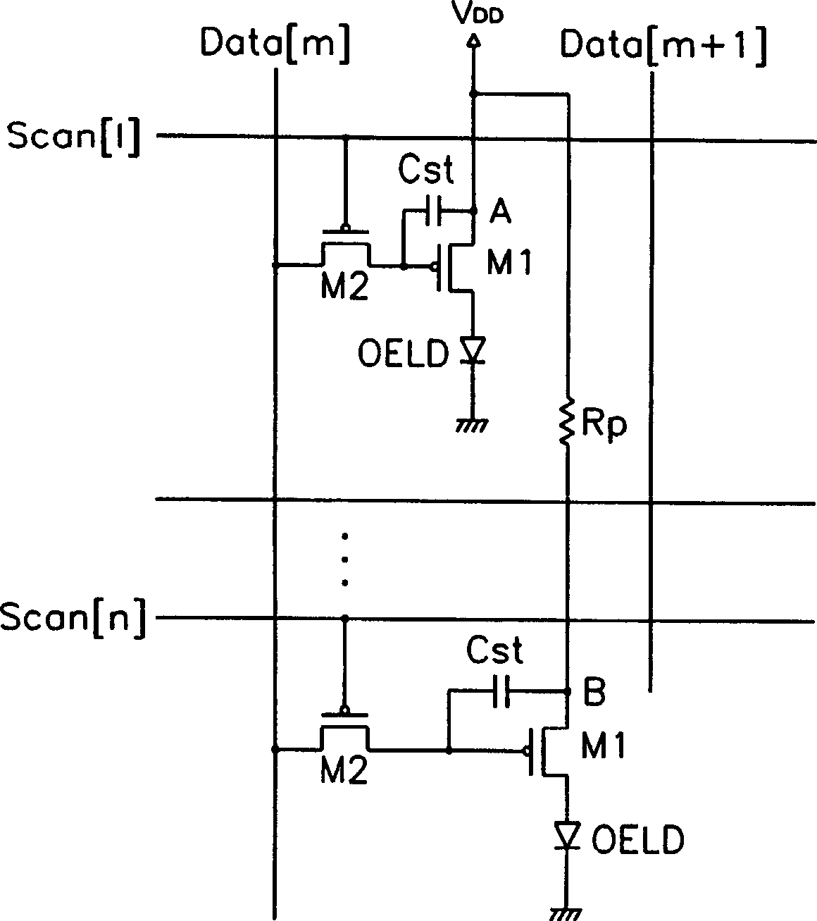
[0033] FIG. 4 shows an organic EL display device according to an embodiment of the present invention.

[0034]As shown in FIG. 4 , an organic EL display device according to an embodiment of the present invention includes an organic EL display panel 10 , a data driver 20 , a scan driver 30 , a timing controller 40 , and a graphic controller 50 .

[0035] The organic EL display panel 10 includes: a plurality of data lines D for transmitting scanning signals 1 、D 2 、D 3 、…D M ;Multiple scan lines S for transmitting scan lines 1 , S 2 , S 3 、…S n ; and a pixel circuit 11 composed of a plurality of pixels determined by data and scan lines.

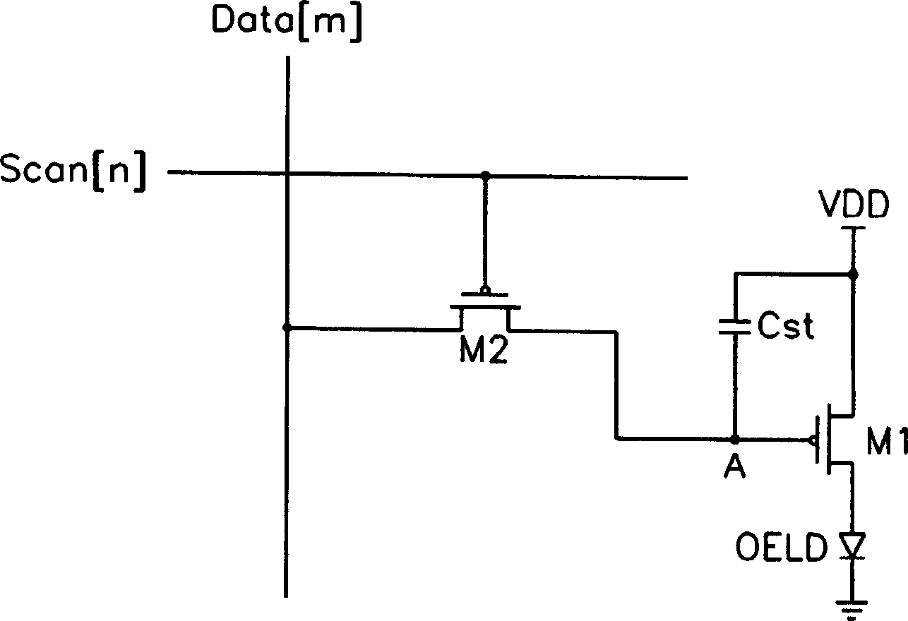
[0036] pixel circuit 11 such as figure 1 The shown may includ...


PUM


Abstract

An organic EL display device and a method for driving the organic EL display device that compensate for a decrease in voltage between the gate and source of a driving transistor caused by a source voltage drop caused by a power supply line resistance. An organic EL display device includes a data driver for receiving digital image data and applying the digital image data and data voltages corresponding to pixel circuits. Even when receiving the same digital image data, the data driver outputs different data voltages according to the positions of the pixel circuits. When the driving transistor is a P-type transistor, the data driver applies a data voltage higher than that applied to a remote pixel circuit to a pixel circuit near an external voltage source even when receiving the same digital data. When the driving transistor is an N-type transistor, the data driver applies a data voltage lower than that applied to a distant pixel circuit to a pixel circuit near an external voltage source even when receiving the same digital data.

Description

technical field [0001] The present invention relates to an organic electroluminescence (hereinafter referred to as EL) display device and a method for driving the organic EL display device. In particular, the present invention relates to an organic EL display device capable of compensating for a voltage drop between the gate and source of a driving transistor caused by a voltage drop of a source voltage caused by a power supply line resistance, and relates to a device for driving A method of an organic EL display device. Background technique [0002] Generally, an organic EL display device is a display device that electrically excites organic fluorescent compounds to emit light, and drives N×M organic fluorescent cells to display images. Techniques for driving organic fluorescent cells include a passive matrix method and an active matrix method using thin film transistors (TFTs). [0003] Compared with the passive matrix method which uses positive and negative electrodes o...

Claims


Application Information

Patent Timeline
Patent Type & Authority Applications(China)
IPC IPC(8): G09G3/30G09G3/32
CPCG09G3/3233G09G2300/0842G09G2310/027G09G2320/0223G09G2320/0233G09G2320/0271G09G2330/02G09G3/30
Inventor 宋俊英李京洙
Owner SAMSUNG DISPLAY CO LTD
Why Eureka
Try Eureka