Optical waveguide equipment and its mfg. method

An optical waveguide and waveguide technology, which is applied to the optical waveguide optical guide, the coupling of the optical waveguide, the optical guide, etc., can solve the problems such as the reduction of the length and the large size of the waveguide of the ring resonator, and achieve the effect of reducing the production cost and reducing the total length.

Inactive Publication Date: 2003-12-10
NEC CORP
View PDF1 Cites 17 Cited by
  • Summary
  • Abstract
  • Description
  • Claims
  • Application Information

AI Technical Summary

Problems solved by technology

Since the above-mentioned optical coupler must have a relatively large size, there is a limit to the reduction of the total waveguide length of the ring resonator 101 or 121.
This constraint limits the maximum frequency at which devices 100 and 120 can operate to approximately 25 GHz

Method used


Image

  • Optical waveguide equipment and its mfg. method
  • Optical waveguide equipment and its mfg. method
  • Optical waveguide equipment and its mfg. method

Examples


no. 1 example

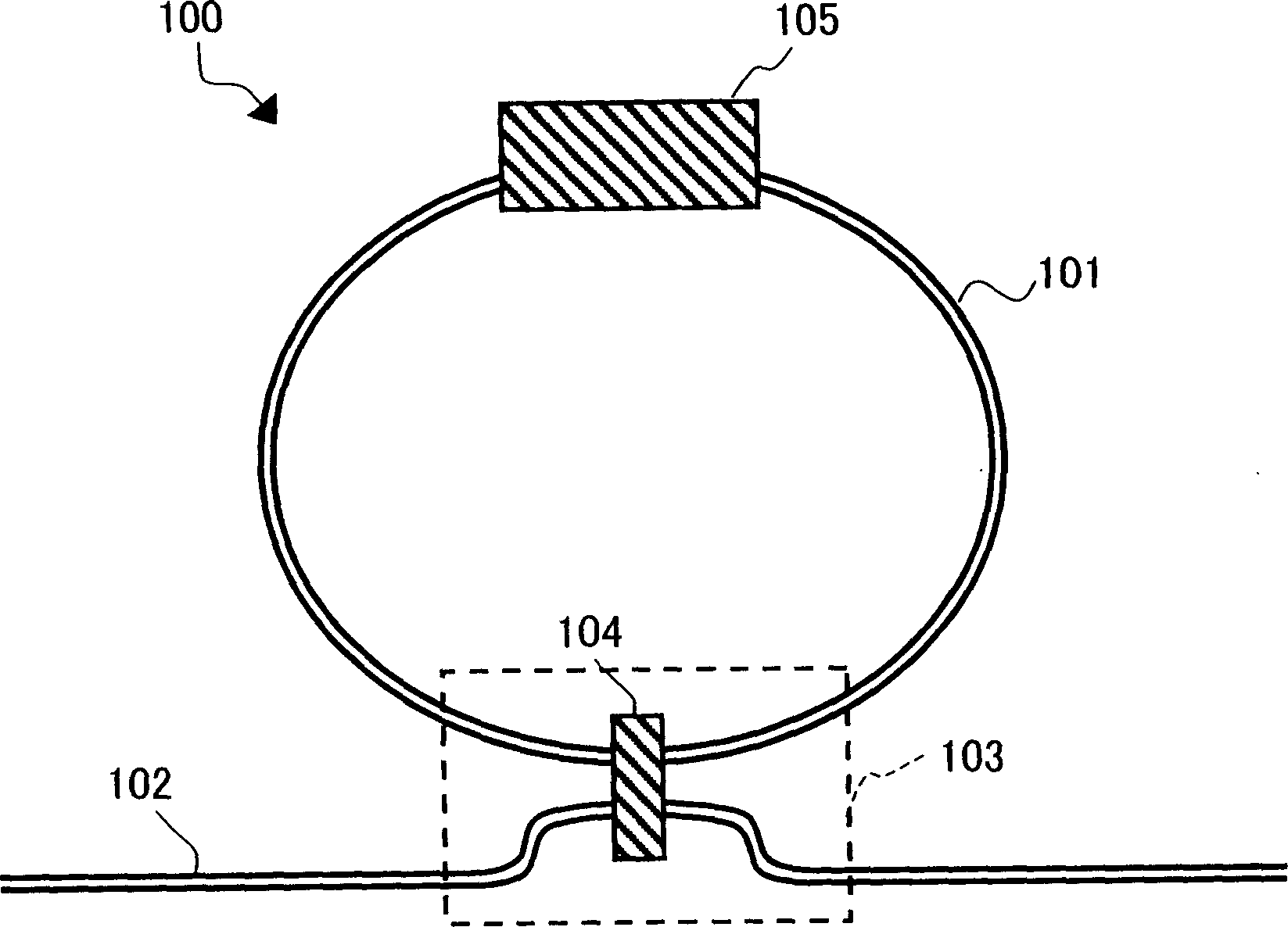
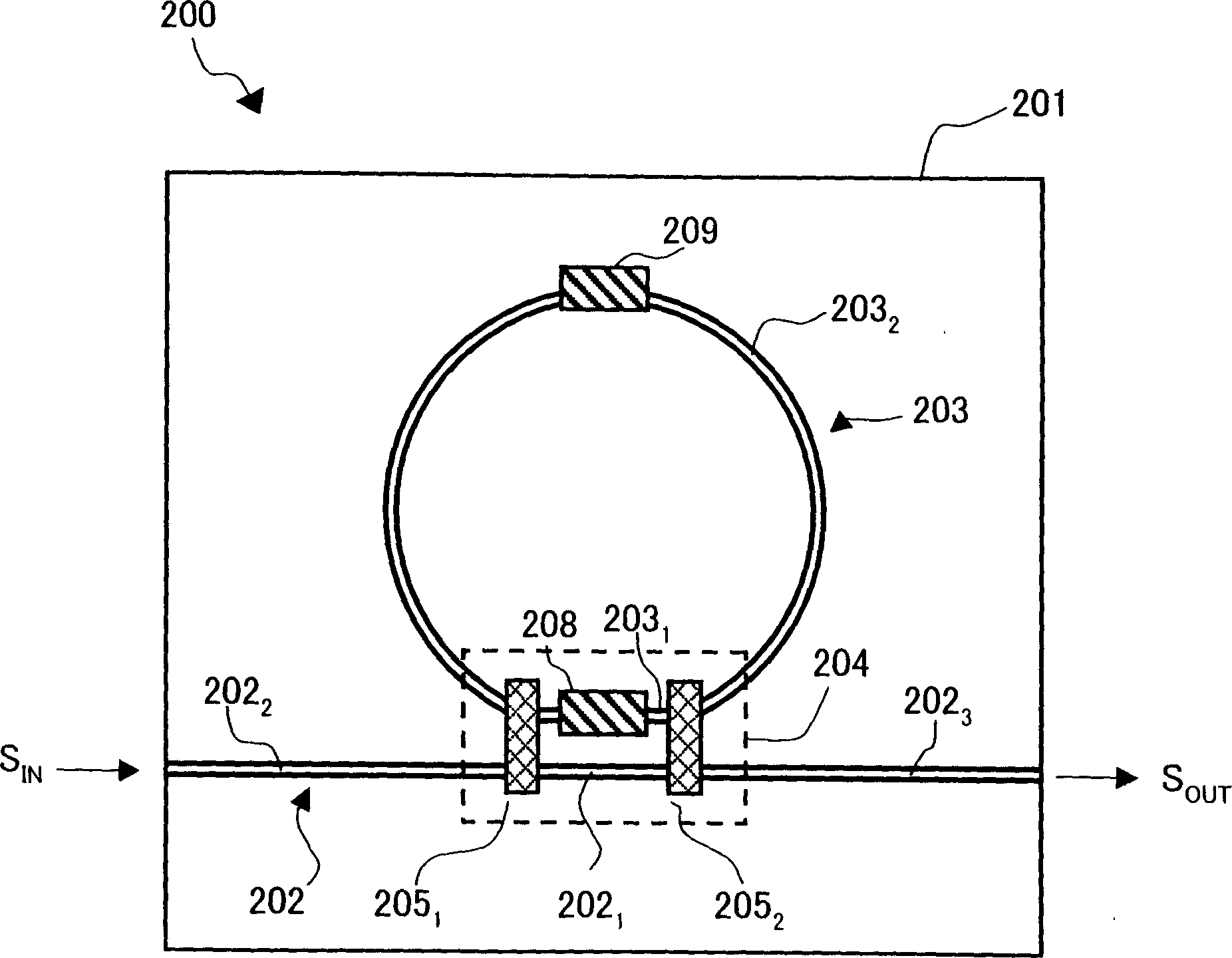
[0150] Such as image 3 As shown, the optical waveguide device 200 according to the first embodiment of the present invention includes an optical waveguide substrate (substrate) 201, a linear optical input / output waveguide 202, a circular or annular optical resonator waveguide 203, and a Mach-Zehnder Interferometer 204 . A linear input / output waveguide 202 , a circular resonator waveguide 203 and an interferometer 204 are all formed on a substrate 201 . The resonator waveguide 203 acts as an optical ring resonator. The interferometer 204 optically connects the input / output waveguide 202 and the resonator waveguide 203 to each other. Here, the device 200 is configured as a kind of optical dispersion compensation device.

[0151] Mach-Zehnder interferometer 204 consists of first and second multi-mode interference (multi-modeinterference, MMI) optical coupler 205 1 and 205 2 and the first and second optical waveguide arms 202 1 and 203 1 composition. The first waveguide a...

no. 2 example

[0195] Figure 7 shows the structure of the optical waveguide device 300 according to the second embodiment of the present invention, each of which is related to image 3 The suffix "A" is added to the same reference symbols used for the first embodiment shown. Same as the first embodiment, the device 300 is configured as a dispersion compensation device.

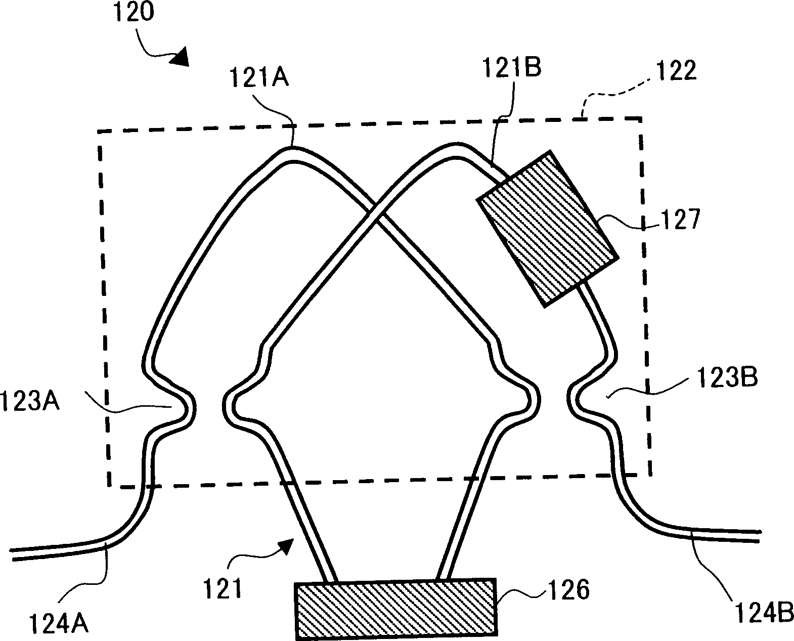
[0196]Specifically, the optical waveguide device 300 according to the second embodiment includes: a cross point or overlap 301 6 curved optical waveguide 301, Mach-Zehnder interferometer 204A, first and second multimode interference optical coupler 205A 1 and 205A 2 , a heater 208A for phase adjustment, and a heater 209A for wavelength adjustment. and in accordance with image 3 The device 200 of the first illustrated embodiment differs in that the input / output optical waveguides and the ring resonator waveguides are not separated from each other. The input / output optical waveguides and the ring resonator waveguides a...

no. 3 example

[0204] Figure 8 shows the structure of the optical waveguide device 400 according to the third embodiment of the present invention, each of which is related to image 3 The suffix "B" is added to the same reference numerals used for the first embodiment shown. Same as the first embodiment, the device 400 is configured as a dispersion compensation device.

[0205] Such as Figure 8 As shown, the optical waveguide device 400 according to the third embodiment includes: a curved optical input / output waveguide 202B, a ring optical resonator waveguide 203B as an optical ring resonator, a Mach-Zehnder interferometer 204B, a phase A heater 208B for tuning, and a heater 209B for wavelength tuning. waveguides 202B and 203B, interferometer 204B, first and second multimode interference coupler 205A 1 , 205A 2 , and the heaters 208B and 209B are formed on the substrate 201 . and Figure 7 The device 300 of the second illustrated embodiment differs in that there is no intersection b...


PUM


Abstract

An optical waveguide device expands the operable frequency range toward the higher frequency side. The device includes a single-mode optical resonator waveguide serving as an optical ring resonator, a single-mode optical input / output waveguide located close to the resonator waveguide in an area, and a Mach-Zehnder interferometer formed in such a way as to include a part of the resonator waveguide as its first optical waveguide arm and a part of the input / output waveguide as its second optical waveguide arm in the area. The interferometer has a first optical coupler for optically coupling the first and second waveguide arms with an input-side part of the input / output waveguide and a remaining part of the resonator waveguide due to multiple-mode optical interference, and a second optical coupler for optically coupling the first and second waveguide arms with an output-side part of the input / output waveguide and the remaining part of the resonator waveguide due to multiple-mode optical interference.

Description

technical field [0001] The invention relates to an optical waveguide device and a manufacturing method thereof. More particularly, the present invention relates to an optical waveguide device using at least one optical ring resonator having an operable or useable frequency range extending towards higher frequencies, and the fabrication of the device method. Background technique [0002] In recent years, the transmission rate of optical fiber communication transmission has been continuously increasing. For example, transmission rates as high as 10 Gbit / s (gigabit / second) have been practically applied in commercial optical fiber communication systems. In addition, in the field of research and development of optical fiber communication, among the reported experimental results, 40Gbit / s, 160Gbit / s and higher transmission rates have been realized in the experiment of optical fiber communication system. [0003] Generally, when the transmission rate increases to 10Gbit / s or hig...

Claims


Application Information

Patent Timeline
Patent Type & Authority Applications(China)
IPC IPC(8): G02B6/12G02B6/122G02B6/34G02F1/01
CPCG02B6/29353G02B6/29343H04B10/25133G02B6/29394G02F1/225
Inventor 山崎裕幸
Owner NEC CORP
Why Eureka
Try Eureka