
Semiconductor memory

A technology of semiconductor and memory, which is applied in the field of semiconductor memory and can solve problems such as effective operation delay

Inactive Publication Date: 2004-03-03
SOCIONEXT INC
View PDF1 Cites 2 Cited by
  • Summary
  • Abstract
  • Description
  • Claims
  • Application Information

AI Technical Summary

Problems solved by technology

Therefore, valid operations to be performed after the flush operation are also delayed

Method used


Image

  • Semiconductor memory
  • Semiconductor memory
  • Semiconductor memory

Examples


Embodiment Construction

[0053] Embodiments of the present invention will now be described with reference to the drawings.

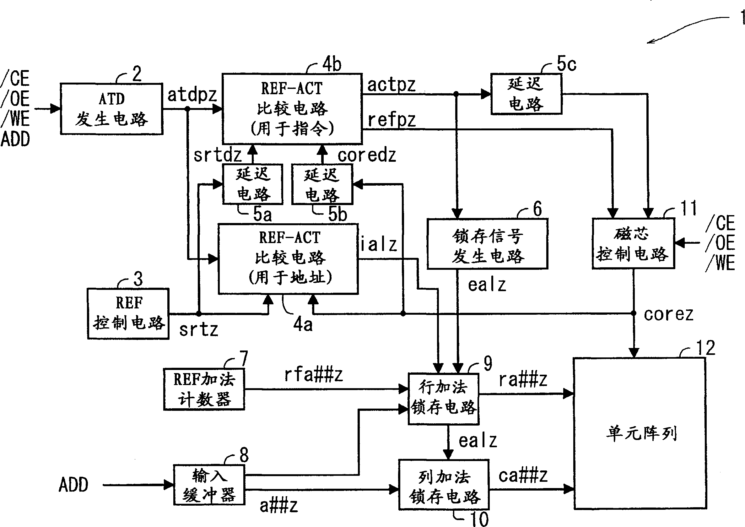
[0054] attached figure 1 Shown is a structural view of a semiconductor memory according to an embodiment of the present invention.

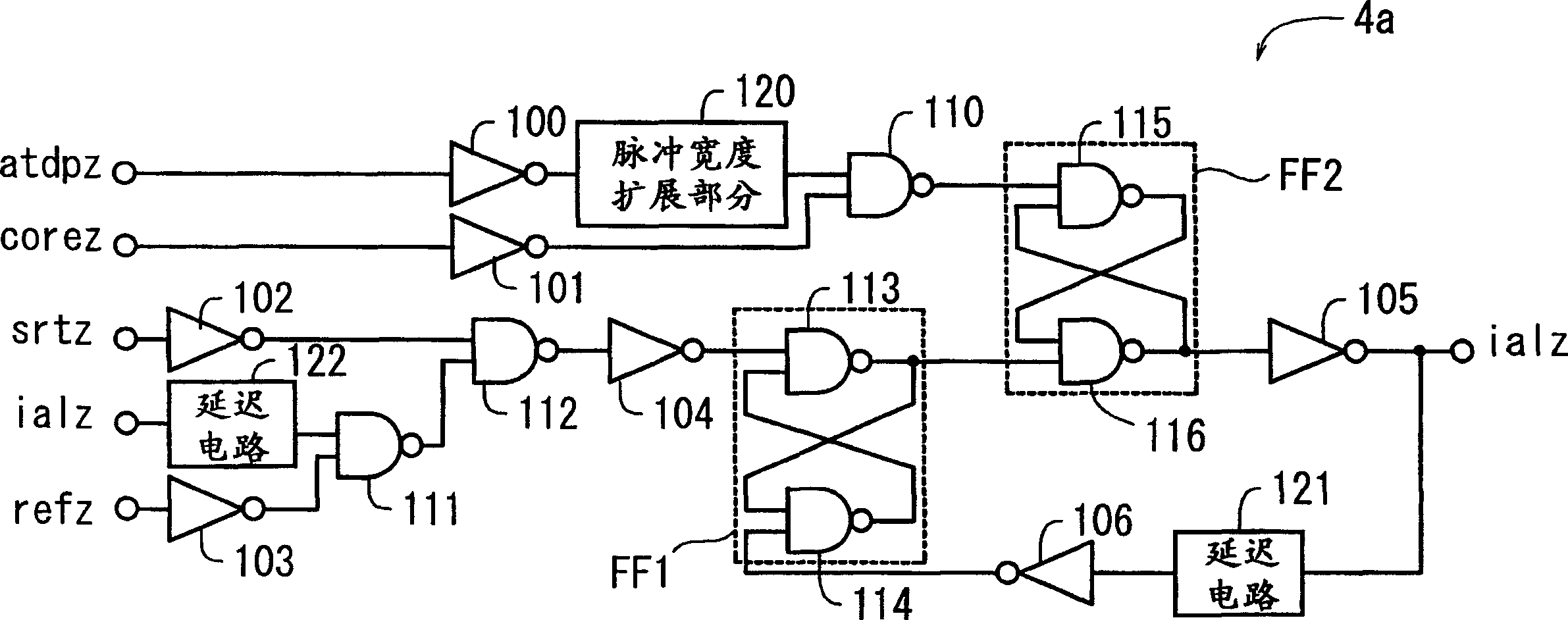
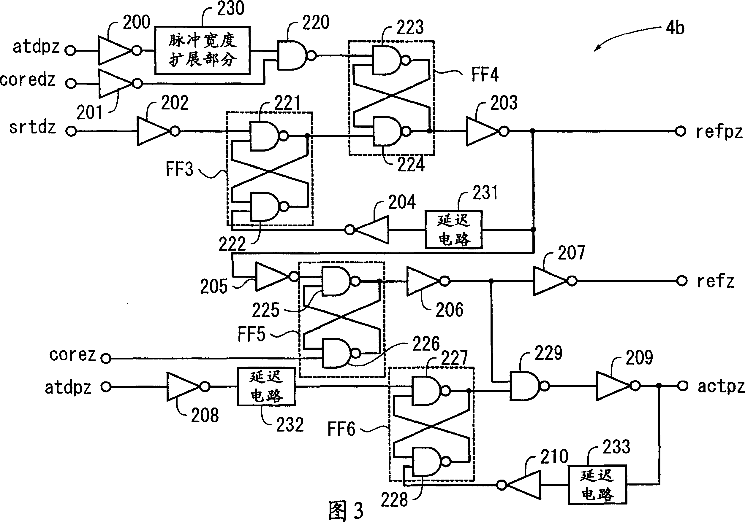
[0055] The semiconductor memory 1 has an ATD generation circuit 2, a REF control circuit 3, REF-ACT comparison circuits 4a and 4b, delay circuits 5a to 5c, a latch signal generation circuit 6, a REF addition counter 7, an input buffer 8, a row addition latch circuit 9, column addition latch circuit 10, core control circuit 11, and memory cell array (core circuit) 12, and has a DRAM structure with an asynchronous SRAM interface in which a refresh operation is automatically performed internally.

[0056] ATD generation circuit 2 detects changes in external signals ( / CE, / WE, / OE and ADD) and generates, for example, an active request signal atdpz representing a read / write request.

[0057] In this case, / CE, / WE, / OE, and ADD are chip enable signal...


PUM


Abstract

A semiconductor memory that shortens refresh operation time. A REF-ACT comparison circuit for addresses compares a refresh request signal srtz and an active request signal atdpz and immediately outputs a refresh address import signal ialz to a row-add latch circuit in the case of the refresh request signal srtz having been input prior to the active request signal atdpz. A REF-ACT comparison circuit for commands compares a delayed refresh request signal srtdz obtained by delaying the refresh request signal srtz and the active request signal atdpz, outputs a refresh execution request signal refpz in the case of the delayed refresh request signal srtdz having been input prior to the active request signal atdpz, and outputs an active execution request signal actpz in the case of the active request signal atdpz having been input prior to the delayed refresh request signal srtdz.

Description

technical field [0001] The present invention relates to a semiconductor memory, and more particularly to a dynamic random access memory (DRAM) type semiconductor memory having an asynchronous static random access memory (SRAM) interface. Background technique [0002] In recent years, DRAM (pseudo-SRAM) with asynchronous SRAM interface has attracted attention due to its low power consumption, feasibility of large storage capacity, and low cost. [0003] For example, Japanese Patent Laid-Open No. 2002-118383 discloses a synchronous pseudo-SRAM that internally performs a refresh operation automatically. [0004] attached Figure 7 Shown is a structural view of a conventional semiconductor memory of pseudo-SRAM type. [0005] The semiconductor memory 20 includes an ATD generation circuit 21, a REF control circuit 22, a REF-ACF comparison circuit 23, delay circuits 24a and 24b, a latch signal generation circuit 25, a REF-addition counter 26, an input buffer 27, a row addition la...

Claims


Application Information

Patent Timeline
Patent Type & Authority Applications(China)
IPC IPC(8): G11C11/402G11C11/403G11C11/406G11C11/408
CPCG11C11/406G11C11/402
Inventor 池田仁史
Owner SOCIONEXT INC
Learn More