Display device and manufacturing method thereof

A display device and one-sided technology, applied in static indicators, nonlinear optics, instruments, etc., can solve the problems of large working voltage, inability to move particles, and increased working voltage, etc., to achieve good display and achieve the effect of displaying spots

Inactive Publication Date: 2004-06-16
PANASONIC CORP
View PDF5 Cites 18 Cited by
  • Summary
  • Abstract
  • Description
  • Claims
  • Application Information

AI Technical Summary

Problems solved by technology

Here, when moving particles between electrodes of opposite polarity according to polarity, the Coulomb force of the electric field provided by the application of the image signal voltage must be greater than the adhesion force (specifically, van der Waals force) between the particles attached to one electrode and the electrode. Or mirror image force) is large, and the particles cannot be drawn away from the electrode and moved to the other electrode. Therefore, a very large operating voltage is required when the display image is transformed.
Therefore, in the display element that further requires the operating voltage of the vibration supply device, the operating voltage is further increased, and if the applied voltage is low, the contrast decreases and display spots occur.

Method used


Image

  • Display device and manufacturing method thereof
  • Display device and manufacturing method thereof
  • Display device and manufacturing method thereof

Examples


Embodiment approach 1

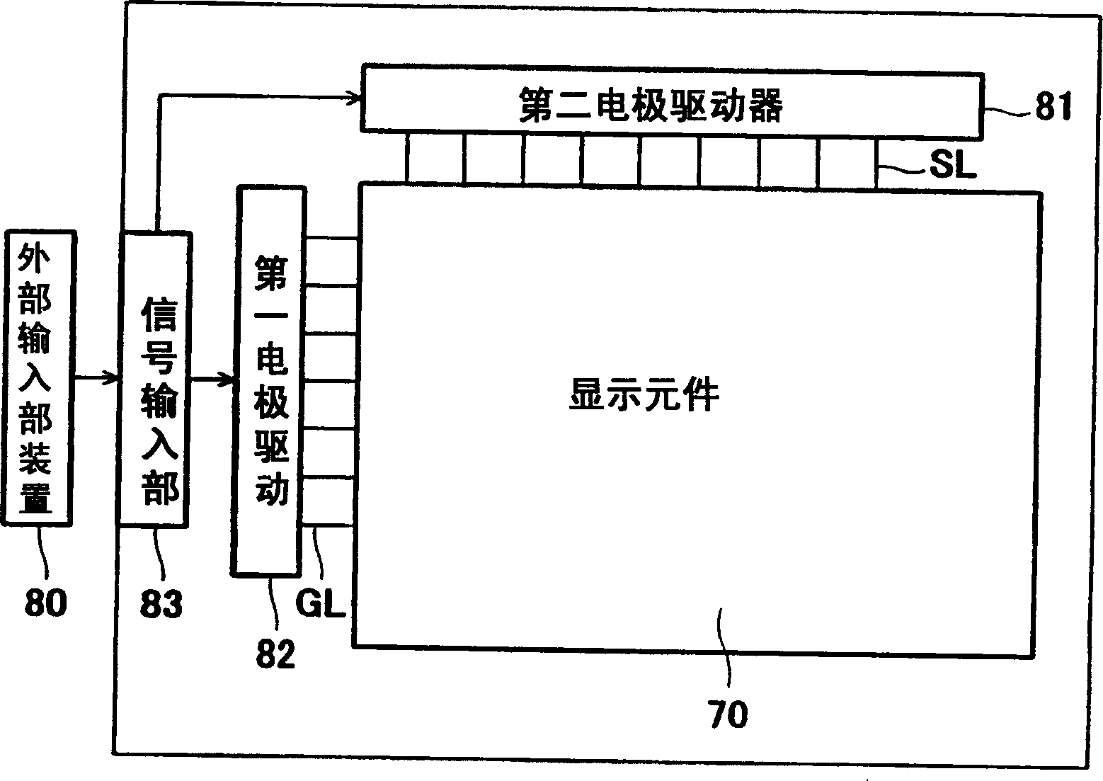
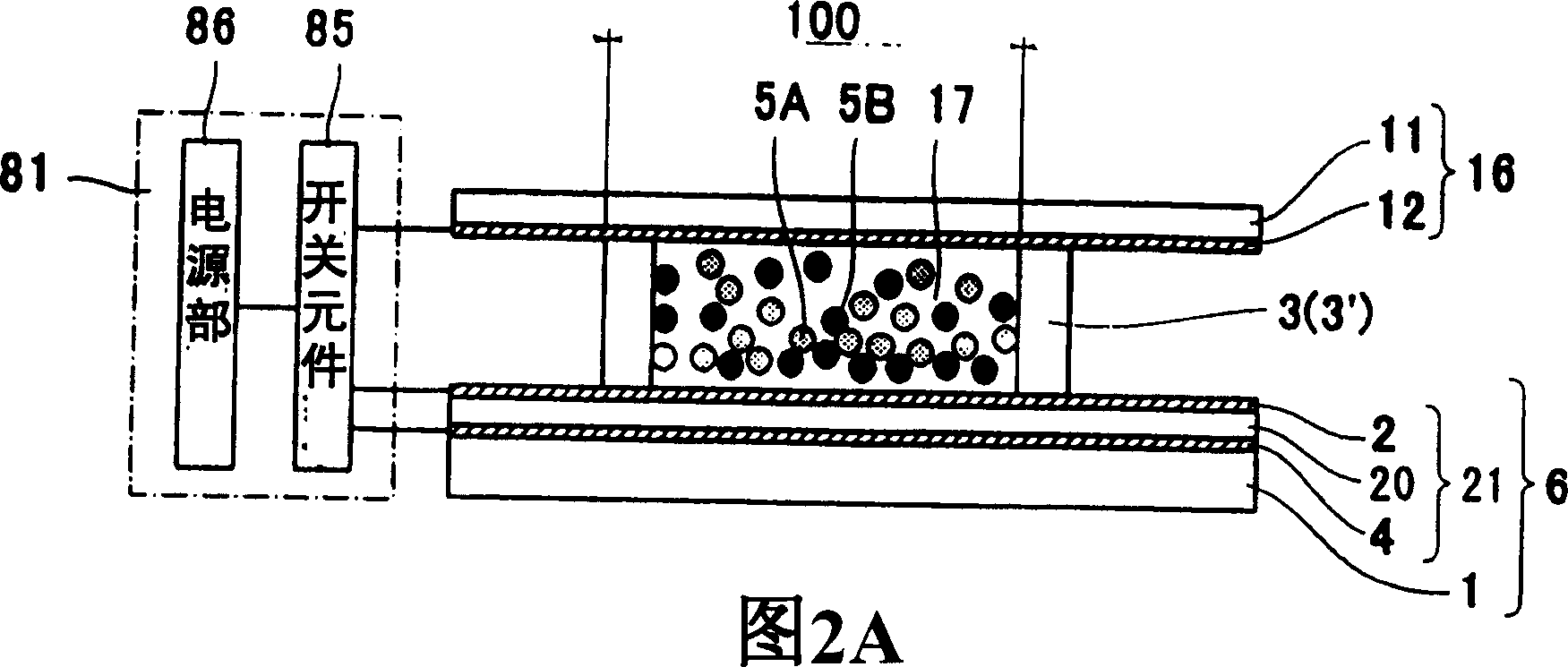
[0108] figure 1 It is a structural schematic diagram of the display device according to Embodiment 1 of the present invention. In addition, Figures 2A-2C are diagrams showing the configuration figure 1 A schematic diagram of a pixel structure of a display element of a display device, showing a cross section perpendicular to the display surface (hereinafter referred to as a vertical cross section).

[0109] Such as figure 1 As shown in FIGS. 2A-2C , the display device is composed of a display element 70 whose display portion is a display panel. As shown in FIGS. 2A-2C , the display element 70 has a lower substrate 6 and an upper substrate 16, and the two substrates 6, 16 are supported by a spacer 3' and are arranged facing each other with a predetermined gap therebetween. Thus, a space 17 is formed between the two substrates 6 , 16 . Since the space 17 is divided by the partition 3', the partition 3' is referred to as the partition wall 3 herein. Each area of ​​the spac...

Embodiment approach 2

[0155] image 3 It is a schematic cross-sectional view showing the structure of a pixel constituting a display element of a display device according to Embodiment 2 of the present invention. Such as image 3 As shown, the display element of this embodiment has the same structure as that of the display element of Embodiment 1, but the difference is that the black particles 5B have conductivity and are formed on the first and second electrodes 2, 12 as a charge transport layer. The electron transport layer 7.

[0156] In Embodiment 1, the case where all the colored particles have insulating properties was described, but if at least one of them is insulating, one of them may be conductive. When the colored particles are conductive, it is necessary to form a thin film or an insulating film containing a charge transport material on the surfaces of the first and second electrodes 2 and 12 that are in contact with the particles. Details are described below.

[0157] For example, ...

Embodiment approach 3

[0162] Figure 4 It is a schematic cross-sectional view showing the structure of a pixel constituting a display element of a display device according to Embodiment 3 of the present invention. Such as Figure 4 As shown, in the display element of the present embodiment, the partition wall 3 functions as the vibration generating portion 21 .

[0163] When making the display element of the present embodiment, for example, use two glass substrates as the first and second substrates 1, 11, and form an ITO film on the surface of each glass substrate respectively, as the first and second electrodes 2, 12, At the same time, polycarbonate films are respectively formed on the ITO films as insulating films 22 . Thus, the upper substrate 16 and the lower substrate 6 are produced.

[0164] Next, on the surface of the prepared lower substrate 6 or upper substrate 16, a sheet-shaped piezoelectric body 20 (hereinafter referred to as a piezoelectric sheet 20) whose front and back surfaces a...


PUM

PropertyMeasurementUnit
thicknessaaaaaaaaaa
thicknessaaaaaaaaaa
thicknessaaaaaaaaaa

Abstract

A lower substrate including a first electrode and an upper substrate including a second electrode are opposed to each other, and a space between the two substrates is partitioned by a partition wall into pixels. In the lower substrate, a piezoelectric material is sandwiched between a third electrode and the first electrode, thereby forming a vibration-generating portion. In the space, negatively charged black particles and positively charged white particles are contained. In a display operation, a signal voltage corresponding to an image signal is applied between the first and second electrodes, generating an electric field, whereby the black particles and the white particles travel between the electrodes and adhere to the respective electrode surfaces to perform the display operation. In rewriting the display, a high-frequency sine wave voltage is applied between the first electrode and the third electrode. Thereby, the piezoelectric material causes a piezoelectric effect, and consequently the vibration-generating portion generates vibration. By transmitting this vibration to the black particles and the white particles, aggregated particles are dissociated and particles adhering to the electrode surfaces are detached therefrom, and these particles are dispersed in the space to erase the display. After erasing the display, a signal voltage corresponding to an image signal is newly applied between the first electrode and the second electrode to perform a display operation.

Description

technical field [0001] The present invention relates to a reversible display device having a display element that performs display by moving a plurality of colored particles by an electric field between a pair of opposing substrates, and a manufacturing method thereof. Background technique [0002] Conventionally, twisted nematic liquid crystal (hereinafter referred to as TN liquid crystal) display devices and organic electroluminescence (hereinafter referred to as organic EL) devices are known as thin, low-power display devices used in portable information terminals. The TN liquid crystal display element changes the alignment state of the liquid crystal molecules in the liquid crystal layer only when a voltage is applied, and thereby controls the transmittance of light passing through the liquid crystal layer to perform display. Therefore, operating power for display is always required, and images cannot be displayed in a power-off state. In addition, since an organic EL e...

Claims


Application Information

Patent Timeline
Patent Type & Authority Applications(China)
IPC IPC(8): G02F1/1343G02F1/167G02F1/1679G09G3/34
CPCG09G2300/0434G09G2310/061G02F1/167G09G3/3493G09G2300/04G09G3/3446G09G3/344G02F1/1679G02F1/1343
Inventor 大植利泰山北裕文河栗真理子
Owner PANASONIC CORP
Why Eureka
Try Eureka