
Film carrying belt for mounting electronic components, production and electrolyzing apparatus

一种电子设备、电镀装置的技术,应用在用电元件组装印刷电路、导电图形的加固、电路等方向,能够解决锡铋合金熔点波动等问题

Inactive Publication Date: 2004-07-07
MITSUI MINING & SMELTING CO LTD
View PDF0 Cites 0 Cited by
  • Summary
  • Abstract
  • Description
  • Claims
  • Application Information

AI Technical Summary

Problems solved by technology

[0011] Substitution between bismuth and tin must be prevented because it causes fluctuations in the melting point of the tin-bismuth alloy

Method used


Image

  • Film carrying belt for mounting electronic components, production and electrolyzing apparatus
  • Film carrying belt for mounting electronic components, production and electrolyzing apparatus
  • Film carrying belt for mounting electronic components, production and electrolyzing apparatus

Examples


example

[0105] According to the following examples, the film carrier tape according to the present invention, the production method therefor and the plating apparatus will be explained in detail. However, it should be noted that the present invention is not limited to the methods of these examples.

example 1

[0107] A polyimide film (UPILEX-S available from UBE INDUSTRUES, LTD.), which has an average thickness of 50 μm, a width of 48 mm, and a length of 120 m, was perforated near the edge portion in the width direction to produce many chain holes.

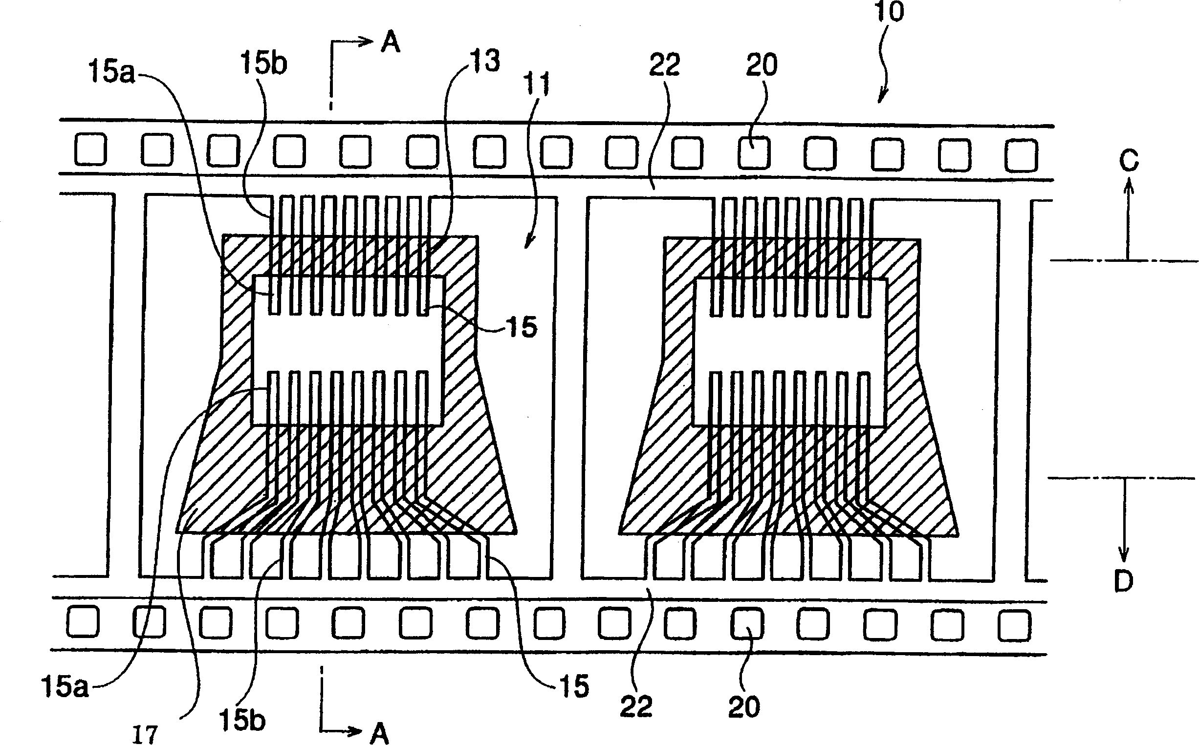
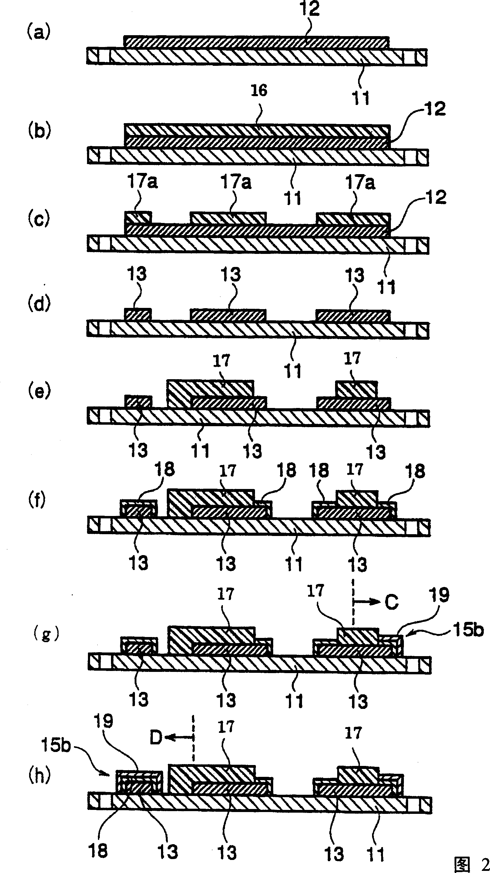
[0108] Thereafter, as shown in FIG. 2( a ), a plated copper foil having an average thickness of 25 μm was bonded on the polyimide film. The electroplated copper foil was covered with photosensitive resin, as shown in Fig. 2(b), and exposed. Developing the exposed resin produces a wiring pattern as shown in FIG. 2(c).

[0109] When the plated copper foil is etched to produce a copper pattern, the resulting pattern is used as a masking material, as shown in Figure 2(d). Using a cleaning base, remove the masking material (exposed resin).

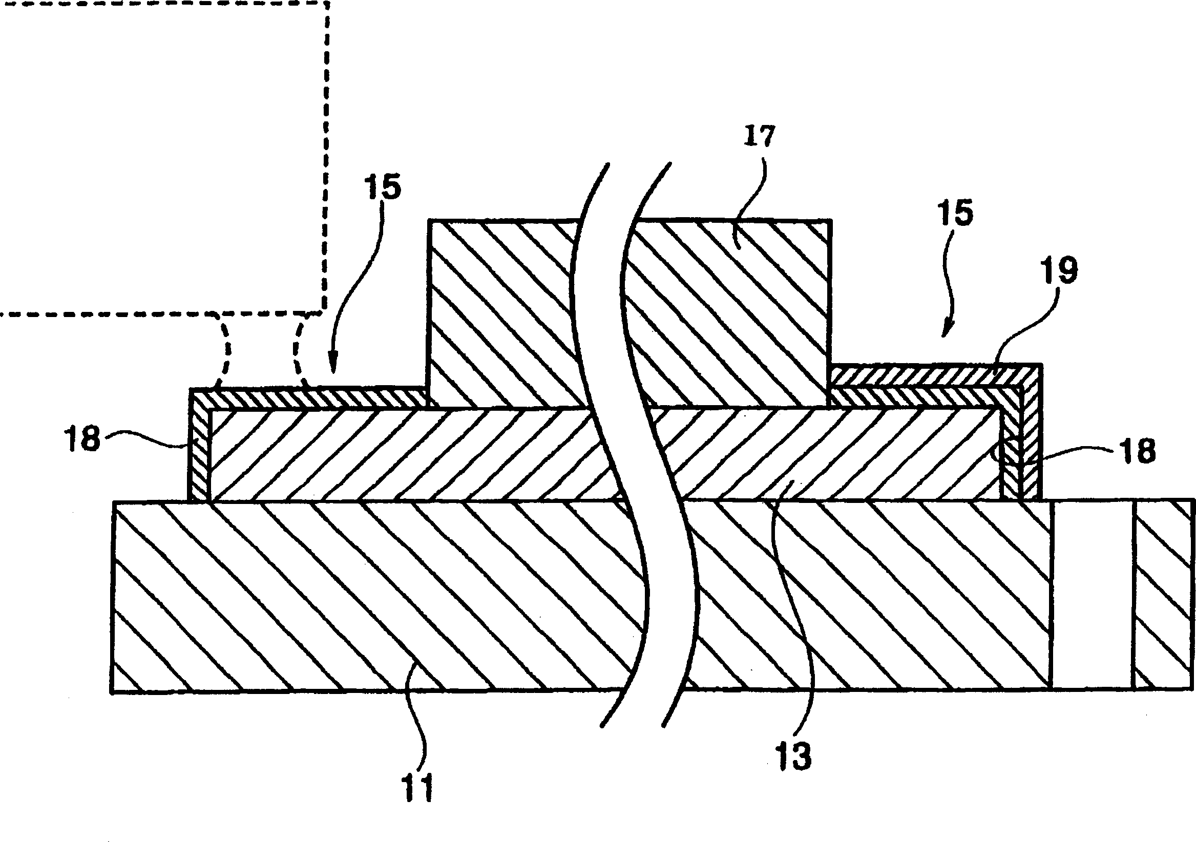
[0110] Then, the entire surface of the wiring pattern is covered with the solder resist solution, except the areas corresponding to the inner and outer leads, as shown in FIG. 2(e). Thereafter, the so...


PUM


Abstract

A film carrier tape for mounting electronic devices thereon has a tin-bismuth alloy deposit in which the bismuth content in the deposit is substantially uniform along a thickness direction thereof. The film carrier tape can be produced by plating at least a part of a wiring pattern with a tin-bismuth alloy and washing the tin-bismuth alloy deposit formed by plating with a water-ejecting washing nozzle within 6 seconds after the plating is completed. A plating apparatus for use in the above production includes a washing nozzle for washing the film carrier tape within 6 seconds after the film carrier tape has exited a plating tank.

Description

technical field [0001] The present invention relates to a thin film carrier tape for mounting electronic equipment, wherein the lead portion is plated with a highly uniform tin-bismuth alloy. The invention also relates to a production method of the film carrier tape and an electroplating device used in the production method. Background technique [0002] A film carrier tape in which many wiring patterns are formed on a flexible insulating film has been used to incorporate electronic equipment into a device. Examples of such film carrier tapes for mounting electronic devices include: TAB (tape automated bonding) tapes, CSP (chip size package: chip size package) tapes, COF (film-based chips: chip on film) tapes , BGA (ball grid array: ball grid array) tape and ASIC (application specific integrated circuit: application specific integrated circuit) tape. These film carrier tapes have inner leads connected to the ends of electronic devices mounted thereon and outer leads connec...

Claims


Application Information

Patent Timeline
Patent Type & Authority Applications(China)
IPC IPC(8): C25D5/48C25D7/00C25D21/08H01L21/48H01L21/60H01L23/498H05K1/00H05K3/24H05K3/34
CPCH01L23/4985H01L2924/0002H05K1/0393H05K3/3463H01L21/4864C25D21/08H05K3/241H05K3/3473H05K2203/1545H01L21/4846H01L23/498C25D5/48H01L2924/00H01L21/60
Inventor 藤本明
Owner MITSUI MINING & SMELTING CO LTD
Learn More