Switching regulator
A technology of regulators and switches, applied in the direction of adjusting electrical variables, control/regulation systems, instruments, etc., can solve problems such as damage to rectifier devices and reduction of input power supply voltage
- Summary
- Abstract
- Description
- Claims
- Application Information
AI Technical Summary
Problems solved by technology
Method used
Image

Examples
no. 1 example
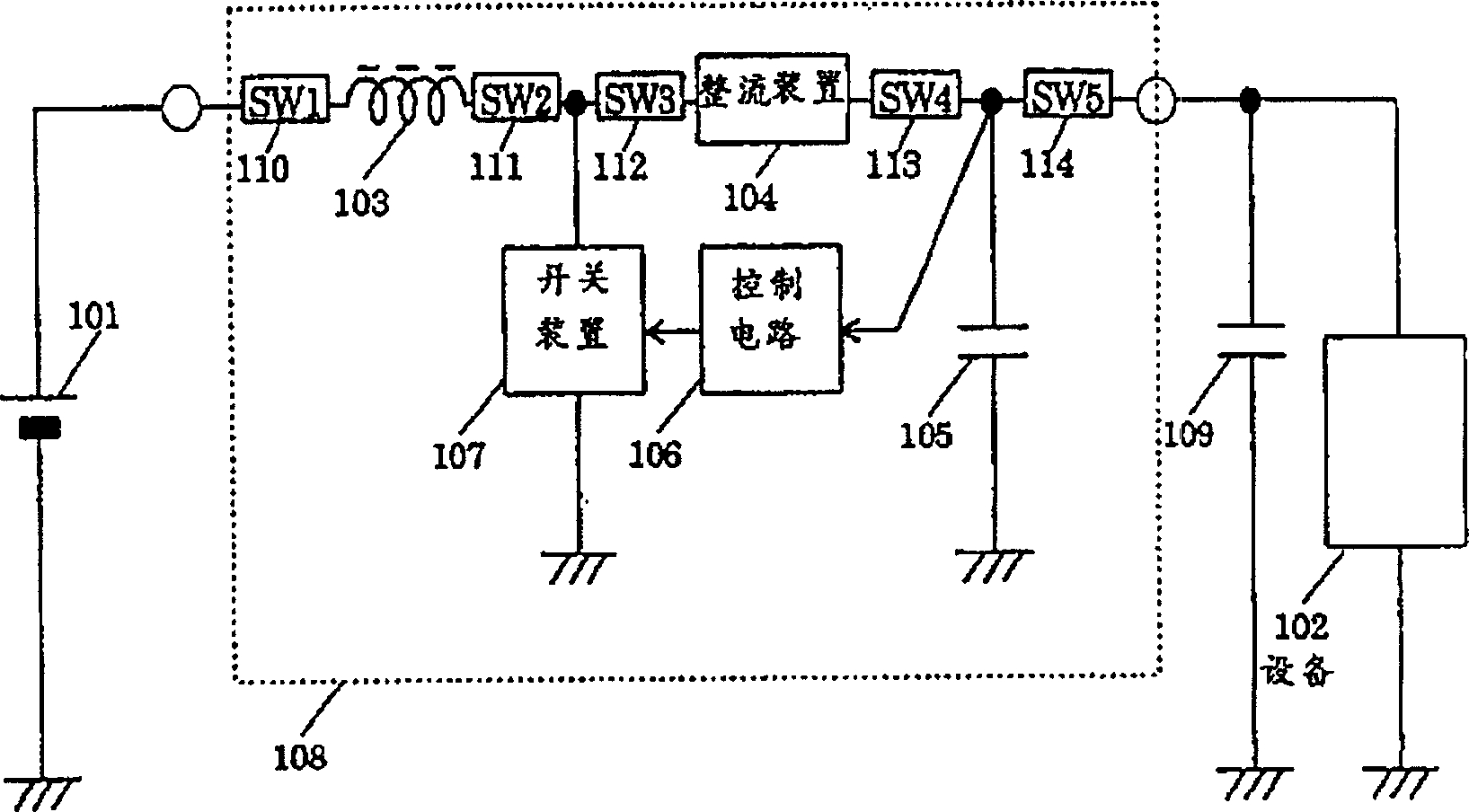
[0021] figure 1 is a schematic diagram showing a chopper-type step-up switching regulator according to a first embodiment of the present invention. In this circuit, the inductor 103, the rectifying device 104, the smoothing capacitor 105, the switching device 107 and the control circuit 106 are the same as the traditional switching regulator. A current limiting switch is employed as one of the switch 110 , the switch 111 , the switch 112 , the switch 113 and the switch 114 located between the input power source 101 and the device 102 . This structure can limit the flow from the input power source 101 to the smoothing capacitor 105 and the device 102 from the stop of the switch-off boost operation between the input power source 101 and the device 102 until the switch-on boost operation starts. The inrush current of capacitor 109.
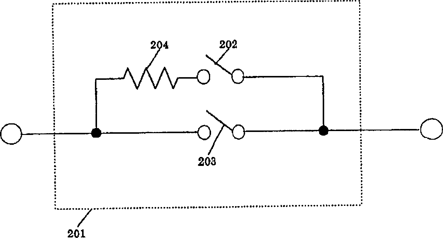
[0022] figure 2 A specific example of a current limiting switch is shown. The switch is composed of a current limiting resistor 204 , a switch...
no. 2 example
[0028] Figure 6 is a circuit diagram showing a chopper switching regulator according to a second embodiment of the present invention. The second embodiment differs from the first embodiment in that the switch can limit the current flowing during a given time interval. Like the first embodiment, Figure 6 This configuration is shown to limit the flow from the input source 601 to the smoothing capacitor 605 and the booster from the time the boost operation is stopped when the switch between the input source 601 and the device 602 is turned off until the boost operation is started when the switch is turned on. Inrush current to capacitor 609 on device 602 .
[0029] Figure 6 A specific example of a switch 610 that can limit the current flowing for a given time is shown. The switch 610 is composed of a transistor 611 , a capacitor 612 , a resistor 613 and a switch 614 . By adding a capacitor 612 and a resistor 613 to the transistor 611 so that the switch 614 can be turned o...
no. 3 example
[0038] Figure 8 is a circuit diagram showing a chopper-type step-up switching regulator according to a third embodiment of the present invention. A current limiting switch is used as in the first embodiment, but this embodiment differs from the first embodiment in the method of current limiting. More specifically, the method uses an inductor 803 placed between the input power source 801 and the device 802, while the switching device 811 and diode 813 are used to control the on / off cycle of time to limit the flow from the input power source 801 to the smoothing capacitor 805 and Inrush current applied to capacitor 809 on device 802.
[0039]Assume that the time period after the switch 811 is turned on is ton, the inductance of the inductor 803 is L, the voltage of the input power supply 814 is VIN, and the output voltage is Vout. The current i flowing into capacitors 805 and 809 is expressed by the following formula:
[0040] i=(VIN-Vout) / L×ton (3)
[0041] As can be seen ...
PUM
 Abstract
Description
Claims
Application Information
 - R&D Engineer
- R&D Manager
- IP Professional
- Industry Leading Data Capabilities
- Powerful AI technology
- Patent DNA Extraction
Browse by: Latest US Patents, China's latest patents, Technical Efficacy Thesaurus, Application Domain, Technology Topic.
© 2024 PatSnap. All rights reserved.Legal|Privacy policy|Modern Slavery Act Transparency Statement|Sitemap