Lithographic apparatus and device manufacturing method
A lithographic projection and component technology, which is used in semiconductor/solid-state device manufacturing, photolithography process exposure devices, microlithography exposure equipment, etc. Problems such as resist T-type topping
- Summary
- Abstract
- Description
- Claims
- Application Information
AI Technical Summary
Problems solved by technology
Method used
Image

Examples
Embodiment 1
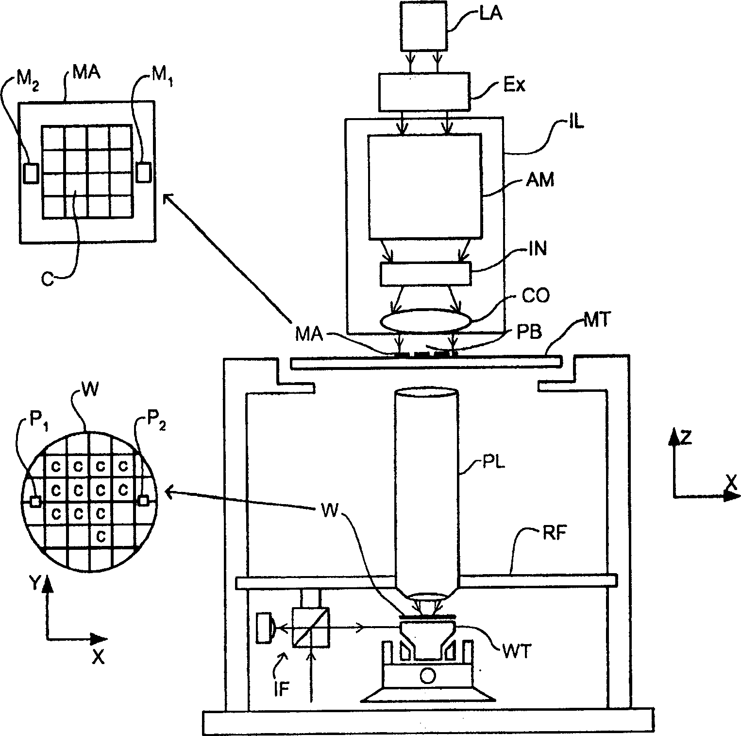
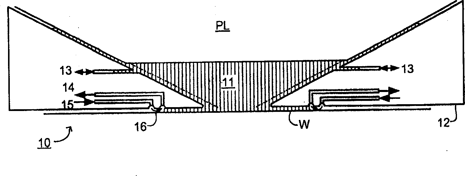
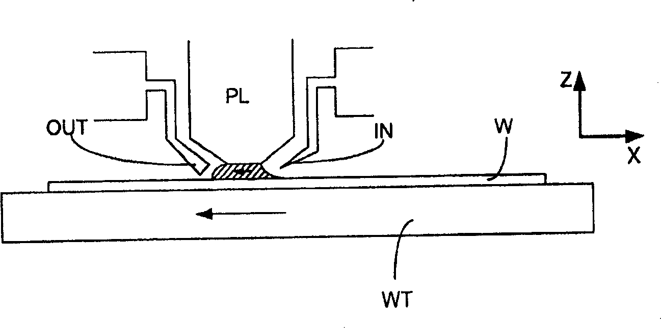
[0041] figure 1 A lithographic projection apparatus according to a specific embodiment of the present invention is schematically shown. The devices include:
[0042] a radiation system Ex, IL, said radiation system Ex, IL for supplying a projection beam PB of radiation such as DUV (deep ultraviolet) radiation, in this particular case the radiation system Ex, IL also comprising a radiation source LA ;
[0043] a first object table (mask table) MT equipped with a mask holder for holding a mask such as a reticle and connected to the first positioning means, the aforementioned first positioning means are used to precisely position the mask relative to the object PL;
[0044] A second object stage (substrate stage) WT equipped with a substrate holder for holding a substrate (for example, a resist-coated silicon wafer) W and connected to on the second positioning device, the above-mentioned second positioning device is used for precise positioning of the substrate relative to t...
PUM
| Property | Measurement | Unit |
|---|---|---|
| Thickness | aaaaa | aaaaa |
Abstract
Description
Claims
Application Information
 - R&D
- Intellectual Property
- Life Sciences
- Materials
- Tech Scout
- Unparalleled Data Quality
- Higher Quality Content
- 60% Fewer Hallucinations
Browse by: Latest US Patents, China's latest patents, Technical Efficacy Thesaurus, Application Domain, Technology Topic, Popular Technical Reports.
© 2025 PatSnap. All rights reserved.Legal|Privacy policy|Modern Slavery Act Transparency Statement|Sitemap|About US| Contact US: help@patsnap.com