Plasma display panel
A plasma and display panel technology, which can be applied to alternating current plasma display panels, solid cathode components, gas discharge tubes/containers, etc., and can solve problems such as reducing luminous efficiency
- Summary
- Abstract
- Description
- Claims
- Application Information
AI Technical Summary
Problems solved by technology
Method used
Image
Examples
Embodiment approach
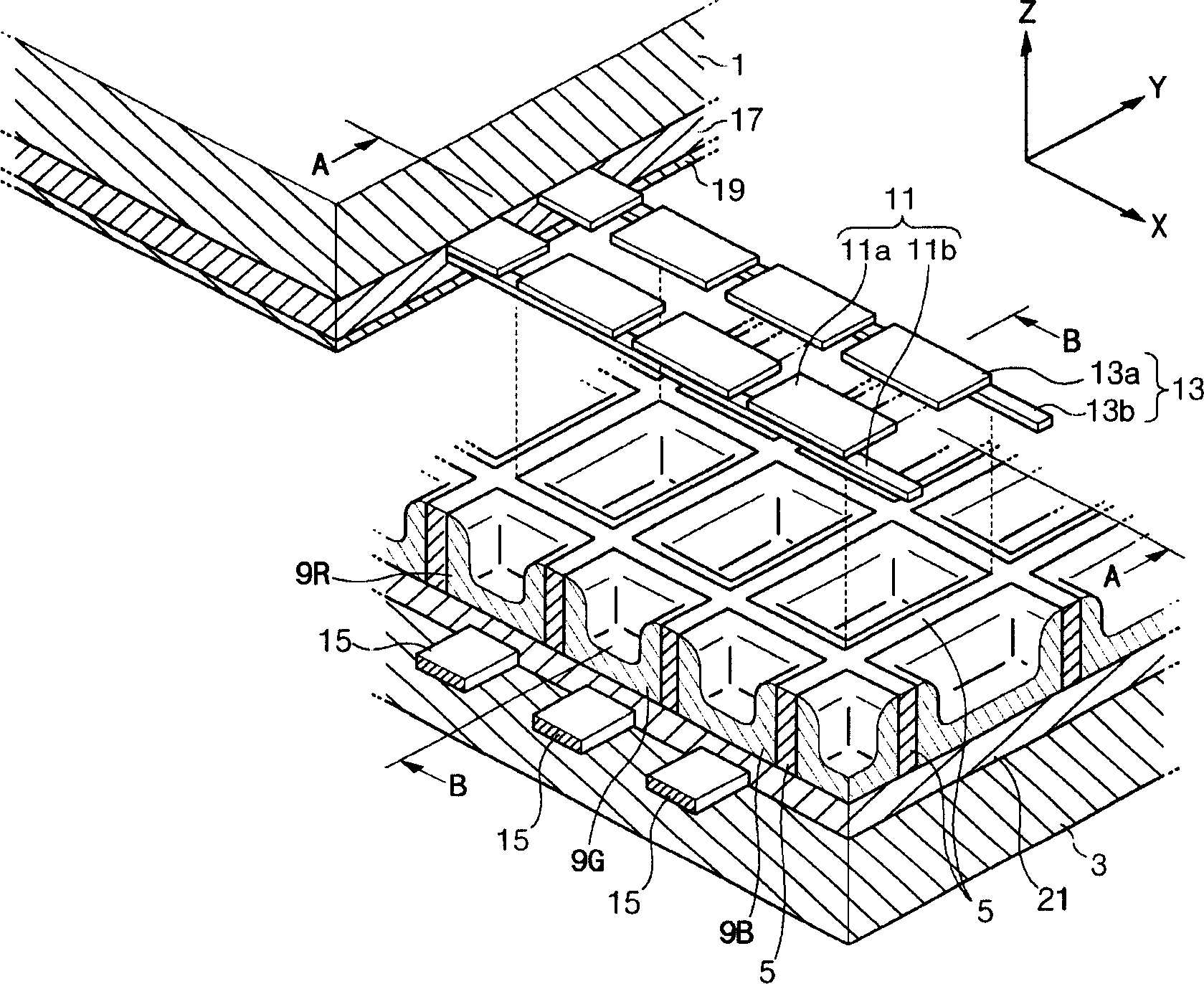
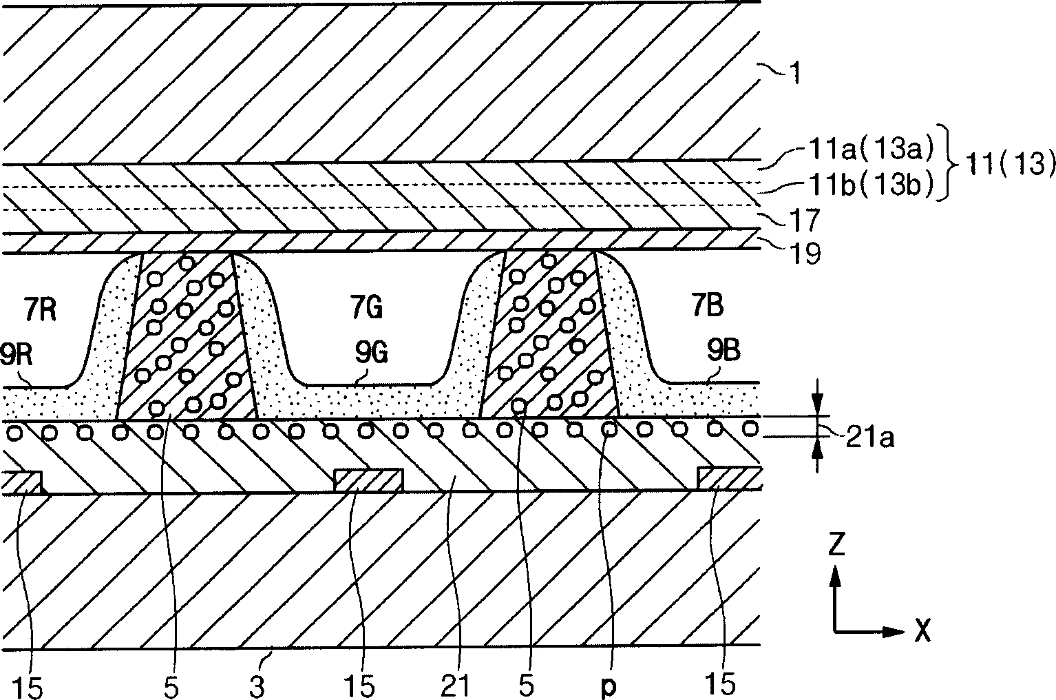
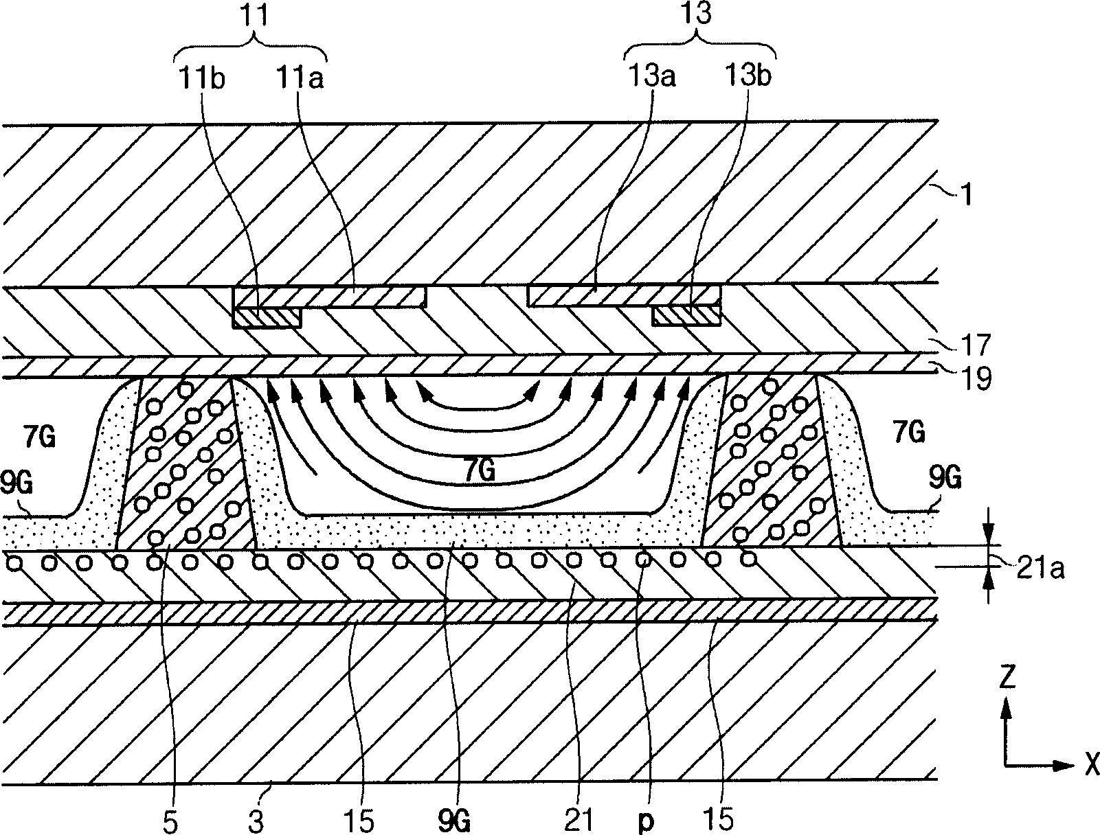
[0042] According to one embodiment, the porous film 21a is formed over the entire area of the dielectric layer 21 based on the X-Y plane direction. According to another embodiment, the porous film 21a is formed only on the portion of the dielectric layer 21 facing the phosphor layers 9R, 9G, 9B excited by vacuum ultraviolet rays.
[0043] According to another embodiment, the porous film 21a is formed over the entire area of the dielectric layer 21 based on the Z-axis direction. According to one embodiment, the porous membrane 21a is formed of a single-layer or double-layer structure. According to one embodiment, the thickness of the porous membrane 21a is about 1 to 2 times larger than the diameter of the phosphor particles, or about the smallest diameter of the void. For example, if the diameter of the phosphor particles is about 3 μm, then the corresponding voids of the porous membrane 21 a may be correspondingly formed with a diameter of about 2 μm to about 4 μm.
[0...
PUM
| Property | Measurement | Unit |
|---|---|---|
| Diameter | aaaaa | aaaaa |
Abstract
Description
Claims
Application Information
 - R&D
- Intellectual Property
- Life Sciences
- Materials
- Tech Scout
- Unparalleled Data Quality
- Higher Quality Content
- 60% Fewer Hallucinations
Browse by: Latest US Patents, China's latest patents, Technical Efficacy Thesaurus, Application Domain, Technology Topic, Popular Technical Reports.
© 2025 PatSnap. All rights reserved.Legal|Privacy policy|Modern Slavery Act Transparency Statement|Sitemap|About US| Contact US: help@patsnap.com


